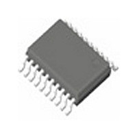
ICS8525BG IDT, Integrated Device Technology Inc, ICS8525BG Datasheet - Page 9

ICS8525BG
Manufacturer Part Number
ICS8525BG
Description
Manufacturer
IDT, Integrated Device Technology Inc
Type
Clock Driverr
Datasheet
1.ICS8525BG.pdf
(13 pages)
Specifications of ICS8525BG
Number Of Clock Inputs
2
Mode Of Operation
Single-Ended
Output Frequency
266MHz
Output Logic Level
LVHSTL
Operating Supply Voltage (min)
3.135V
Operating Supply Voltage (typ)
3.3V
Operating Supply Voltage (max)
3.465V
Package Type
TSSOP
Operating Temp Range
0C to 70C
Operating Temperature Classification
Commercial
Signal Type
LVCMOS/LVTTL
Mounting
Surface Mount
Pin Count
20
Lead Free Status / RoHS Status
Not Compliant
ICS8525
L
S
, 1-
-4
OW
KEW
TO
LVCMOS-
-LVHSTL F
B
TO
ANOUT
UFFER
3. Calculations and Equations.
The purpose of this section is to derive the power dissipated into the load.
LVHSTL output driver circuit and termination are shown in Figure 2.
V
DDO
Q1
V
OUT
RL
50
F
2. LVHSTL D
C
T
IGURE
RIVER
IRCUIT AND
ERMINATION
To calculate worst case power dissipation into the load, use the following equations which assume a 50 load.
Pd_H is power dissipation when the output drives high.
Pd_L is the power dissipation when the output drives low.
Pd_H = (V
/R
) * (V
- V
)
OH_MIN
L
DDO_MAX
OH_MIN
Pd_L = (V
/R
) * (V
- V
)
OL_MAX
L
DDO_MAX
OL_MAX
Pd_H = (1V/50 ) * (2V - 1V) = 20mW
Pd_L = (0.4V/50 ) * (2V - 0.4V) = 12.8mW
Total Power Dissipation per output pair = Pd_H + Pd_L = 32.8mW
www.icst.com/products/hiperclocks.html
8525BG
REV. C AUGUST 1, 2007
9


