IDTMPC9446FA IDT, Integrated Device Technology Inc, IDTMPC9446FA Datasheet
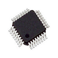
IDTMPC9446FA

Manufacturer Part Number
IDTMPC9446FA
Description
Manufacturer
IDT, Integrated Device Technology Inc
Type
Clock Dividerr
Datasheet

Specifications of IDTMPC9446FA

Number Of Clock Inputs
2
Mode Of Operation
Single-Ended
Output Frequency
250MHz
Output Logic Level
LVCMOS
Operating Supply Voltage (min)
2.375V
Operating Supply Voltage (typ)
2.5/3.3V
Operating Supply Voltage (max)
3.465V
Package Type
TQFP
Operating Temp Range
-40C to 85C
Operating Temperature Classification
Industrial
Signal Type
LVCMOS
Mounting
Surface Mount
Pin Count
32
Quiescent Current
2mA
Lead Free Status / RoHS Status
Not Compliant
for low-voltage mid-range to high-performance telecom, networking and computing
applications. Both 3.3 V, 2.5 V and dual supply voltages are supported for mixed-voltage
applications. The MPC9446 offers 10 low-skew outputs and 2 selectable inputs for clock
redundancy. The outputs are configurable and support 1:1 and 1:2 output to input
frequency ratios. The MPC9446 is specified for the extended temperature range of –40°C
to 85°C.
Features
Functional Description
250 MHz. The signals are generated and retimed on-chip to ensure minimal skew be-
tween the three output banks. Two independent LVCMOS compatible clock inputs are available. This feature supports redundant clock
sources or the addition of a test clock into the system design. Each of the three output banks can be individually supplied by 2.5 V or 3.3
V supporting mixed voltage applications. The FSELx pins choose between division of the input reference frequency by one or two. The
frequency divider can be set individually for each of the three output banks. The MPC9446 can be rese,t and the outputs are disabled by
deasserting the MR/OE pin (logic high state). Asserting MR/OE will enable the outputs.
transmission lines. Please consult the MPC9456 specification for a 1:10 mixed voltage buffer with LVPECL compatible inputs. For series
terminated transmission lines, each of the MPC9446 outputs can drive one or two traces giving the devices an effective fanout of 1:20.
The device is packaged in a 7x7 mm
3.3V AND 2.5V, LVCMOS CLOCK FANOUT BUFFER
IDT™ / ICS™ LVCMOS CLOCK FANOUT BUFFER
The MPC9446 is a 2.5 V and 3.3 V compatible 1:10 clock distribution buffer designed
The MPC9446 is a full static fanout buffer design supporting clock frequencies up to
All inputs accept LVCMOS signals while the outputs provide LVCMOS compatible levels with the capability to drive terminated 50 Ω
Configurable 10 outputs LVCMOS clock distribution buffer
Compatible to single, dual and mixed 3.3 V/2.5 V voltage supply
Designed for mid-range to high-performance telecom, networking
and computer applications
Supports applications requiring clock redundancy
Maximum output skew of 200 ps (150 ps within one bank)
Selectable output configurations per output bank
Tristable outputs
32-lead LQFP package
32-lead Pb-free package available
Ambient operating temperature range of –40 to 85°C
Wide range output clock frequency up to 250 MHz
2
32-lead LQFP package.
1
DUAL SUPPLY 2.5 V AND 3.3 V
LOW VOLTAGE SINGLE OR
DISTRIBUTION BUFFER
32-LEAD LQFP PACKAGE
MPC9446REV 4 NOVEMBER 28, 2007
Pb-FREE PACKAGE
LVCMOS CLOCK
MPC9446
CASE 873A-04
CASE 873A-04
FA SUFFIX
AC SUFFIX
MPC9446

Related parts for IDTMPC9446FA

IDTMPC9446FA Summary of contents

Page 1

AND 2.5V, LVCMOS CLOCK FANOUT BUFFER The MPC9446 is a 2.5 V and 3.3 V compatible 1:10 clock distribution buffer designed for low-voltage mid-range to high-performance telecom, networking and computing applications. Both 3.3 V, 2.5 V and dual supply ...

Page 2

MPC9446 3.3V AND 2.5V LVCMOS CLOCK FANOUT BUFFER CCLK0 CCLK1 CCLK_SEL FSELA FSELB FSELC MR/OE V CCA QA2 GND QA1 V CCA QA0 GND MR/OE Figure 2. Pinout: 32-Lead Package Pinout (Top View) IDT™ / ICS™ LVCMOS CLOCK FANOUT BUFFER ...

Page 3

MPC9446 3.3V AND 2.5V LVCMOS CLOCK FANOUT BUFFER Table 1. Pin Configuration Pin I/O CCLK0,1 Input FSELA, FSELB, FSELC Input MR/OE Input GND ( CCA CCB CCC V CC QA0 – QA2 Output QB0 – ...

Page 4

MPC9446 3.3V AND 2.5V LVCMOS CLOCK FANOUT BUFFER Table 5. General Specifications Symbol Characteristics V Output Termination Voltage TT MM ESD Protection (Machine Model) HBM ESD Protection (Human Body Model) LU Latch-Up Immunity C Power Dissipation Capacitance PD C Input ...

Page 5

MPC9446 3.3V AND 2.5V LVCMOS CLOCK FANOUT BUFFER Table 8. DC Characteristics ( Symbol Characteristics V Input High Voltage IH V Input Low Voltage IL V Output High Voltage OH V Output Low Voltage OL Z Output ...

Page 6

MPC9446 3.3V AND 2.5V LVCMOS CLOCK FANOUT BUFFER Driving Transmission Lines The MPC9446 clock driver was designed to drive high- speed signals in a terminated transmission line environment. To provide the optimum flexibility to the user, the output drivers were ...

Page 7

MPC9446 3.3V AND 2.5V LVCMOS CLOCK FANOUT BUFFER Pulse Generator Z = 50Ω Figure 6. CCLK0, 1 MPC9446 AC Test Reference for Figure 7. Output Transition Time Test Reference t SK(LH) The pin-to-pin skew is ...

Page 8

MPC9446 3.3V AND 2.5V LVCMOS CLOCK FANOUT BUFFER IDT™ / ICS™ LVCMOS CLOCK FANOUT BUFFER PACKAGE DIMENSIONS CASE 873A-04 ISSUE C 32-LEAD LQFP PACKAGE PAGE 8MPC9446 REV 4 NOVEMBER 28, 2007) ...

Page 9

MPC9446 3.3V AND 2.5V LVCMOS CLOCK FANOUT BUFFER IDT™ / ICS™ LVCMOS CLOCK FANOUT BUFFER PACKAGE DIMENSIONS CASE 873A-04 ISSUE C 32-LEAD LQFP PACKAGE PAGE 9MPC9446 REV 4 NOVEMBER 28, 2007) ...

Page 10

MPC9446 3.3V AND 2.5V LVCMOS CLOCK FANOUT BUFFER IDT™ / ICS™ LVCMOS CLOCK FANOUT BUFFER PACKAGE DIMENSIONS CASE 873A-04 ISSUE C 32-LEAD LQFP PACKAGE PAGE 10MPC9446 REV 4 NOVEMBER 28, 2007) ...

Page 11

MPC9446 3.3V AND 2.5V LVCMOS CLOCK FANOUT BUFFER Innovate with IDT and accelerate your future networks. Contact: www.IDT.com For Sales For Tech Support 800-345-7015 netcom@idt.com 408-284-8200 480-763-2056 Fax: 408-284-2775 Corporate Headquarters Asia Pacific and Japan Integrated Device Technology, Inc. Integrated ...

Related keywords