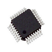
IDTMPC9448FA IDT, Integrated Device Technology Inc, IDTMPC9448FA Datasheet - Page 4

IDTMPC9448FA
Manufacturer Part Number
IDTMPC9448FA
Description
Manufacturer
IDT, Integrated Device Technology Inc
Type
Clock Driverr
Datasheet
1.IDTMPC9448FA.pdf
(12 pages)
Specifications of IDTMPC9448FA
Number Of Clock Inputs
2
Output Frequency
350MHz
Output Logic Level
LVCMOS
Operating Supply Voltage (min)
2.375V
Operating Supply Voltage (typ)
2.5/3.3V
Operating Supply Voltage (max)
3.465V
Package Type
TQFP
Operating Temp Range
-40C to 85C
Operating Temperature Classification
Industrial
Signal Type
LVCMOS/LVPECL
Mounting
Surface Mount
Pin Count
32
Quiescent Current
2mA
Lead Free Status / RoHS Status
Not Compliant
Available stocks
Company
Part Number
Manufacturer
Quantity
Price
Company:
Part Number:
IDTMPC9448FA
Manufacturer:
IDT
Quantity:
7 209
IDT™ 3.3 V/2.5 V LVCMOS 1:12 Clock Fanout Buffer
Freescale Timing Solutions Organization has been acquired by Integrated Device Technology, Inc
IDT™ / ICS™ LVCMOS 1:12 CLOCK FANOUT BUFFER
MPC9448
3.3 V/2.5 V LVCMOS 1:12 Clock Fanout Buffer
Table 6. AC Characteristics (V
Table 7. DC Characteristics (V
MPC9448
3.3V/2.5V LVCMOS 1:12 CLOCK FANOUT BUFFER
1. AC characteristics apply for parallel output termination of 50 Ω to V
2. V
3. Violation of the 1.0 ns maximum input rise and fall time limit will affect the device propagation delay, device-to-device skew, reference input
4. Output pulse skew is the absolute difference of the propagation delay times: | t
Symbol
1. V
2. Input pull-up / pull-down resistors influence input current.
3. The MPC9448 is capable of driving 50 Ω transmission lines on the incident edge. Each output drives one 50 Ω parallel terminated
4. I
V
I
CCQ
Z
Symbol
V
CMR
t
V
t
V
V
t
t
t
V
PLZ, HZ
t
V
PLH/HL
PLH/HL
PZL, LZ
and the input swing lies within the V
pulse width, output duty cycle and maximum frequency specifications.
I
OUT
and the input swing lies within the V
transmission line to a termination voltage of V
V
P, REF
t
CMR
t
f
sk(PP)
DC
OH
CCQ
SK(P)
PP
IN
OL
V
sk(O)
t
t
IH
MAX
IL
f
CMR
CMR
CC
r
r
t
t
ref
PP
, t
, t
S
H
(4)
(1)
Q
f
f
(2)
= 2.5 V.
is the DC current consumption of the device with all outputs open and the input in its default state or open.
(AC) is the crosspoint of the differential input signal. Normal AC operation is obtained when the crosspoint is within the V
(DC) is the crosspoint of the differential input signal. Functional operation is obtained when the crosspoint is within the V
Input high voltage
Input low voltage
Peak-to-peak input voltage
Common Mode Range
Input current
Output High Voltage
Output Low Voltage
Output impedance
Maximum Quiescent Supply Current
Input Frequency
Maximum Output Frequency
Peak-to-Peak Input Voltage
Common Mode Range
Reference Input Pulse Width
CCLK Input Rise/Fall Time
Propagation Delay
Output Disable Time
Output Enable Time
Setup Time
Hold Time
Output-to-Output Skew
Device-to-Device Skew
Output Pulse skew
Output Duty Cycle
Output Rise/Fall Time
(2)
Characteristics
(4)
CC
Characteristics
CC
= 3.3 V ± 5%, T
= 2.5 V ± 5%, T
PP
PP
(AC) specification. Violation of V
(DC) specification.
PCLK or CCLK to any Q
TT
CCLK to CLK_STOP
CCLK to CLK_STOP
PCLK to CLK_STOP
PCLK to CLK_STOP
. Alternatively, the device drives one 50 Ω series terminated transmission lines at
PCLK
PCLK
A
CCLK to any Q
PCLK to any Q
A
= -40°C to +85°C)
= -40°C to +85°C)
Using CCLK
Using PCLK
f
Q
<170 MHz
PCLK
PCLK
–0.3
Min
250
1.7
1.0
1.8
TT
4
4
.
CMR
Min
400
1.3
1.4
1.6
1.3
0.0
0.0
1.0
1.5
0.1
45
(1)
0
0
or V
pLH
Typ
19
PP
– t
impacts t
pHL
Typ
|.
50
V
V
PLH/HL
CC
CC
Max
300
0.7
0.6
2.0
+ 0.3
– 0.7
V
and t
CC
1.0
1000
Max
350
350
150
300
400
3.6
3.3
2.0
1.0
11
11
55
– 0.8
(3)
SK(PP)
Unit
mV
mA
μA
Ω
V
V
V
V
V
MPC9448
.
MHz
MHz
Unit
LVCMOS
LVCMOS
LVPECL
LVPECL
V
I
I
All V
mV
OH
OL
ns
ns
ns
ns
ns
ns
ns
ns
ns
ns
ps
ns
ps
ps
ns
%
V
IN
= 15 mA
= –15 mA
= GND or V
CC
Condition
LVPECL
LVPECL
0.8 to 2.0 V
DC
0.55 to 2.4 V
Pins
REV 6 JULY 11, 2006
REF
Condition
(3)
CMR
CMR
(3)
= 50%
IN
range
= V
range
NETCOM
CC
MPC9448


