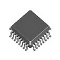
83940BYLF IDT, Integrated Device Technology Inc, 83940BYLF Datasheet - Page 7

83940BYLF
Manufacturer Part Number
83940BYLF
Description
Manufacturer
IDT, Integrated Device Technology Inc
Type
Clock Driverr
Datasheet
1.83940BYLF.pdf
(13 pages)
Specifications of 83940BYLF
Number Of Clock Inputs
2
Output Frequency
250MHz
Output Logic Level
LVCMOS/LVTTL
Operating Supply Voltage (min)
2.375V
Operating Supply Voltage (typ)
2.5/3.3V
Operating Supply Voltage (max)
3.465V
Package Type
LQFP
Operating Temp Range
0C to 70C
Operating Temperature Classification
Commercial
Mounting
Surface Mount
Pin Count
32
Lead Free Status / RoHS Status
Compliant
W
Figure 1 shows how the differential input can be wired to accept
single ended levels. The reference voltage V_REF = V
generated by the bias resistors R1, R2 and C1. This bias circuit
should be located as close as possible to the input pin. The ratio
83940BY
IRING THE
D
IFFERENTIAL
I
F
NPUT TO
IGURE
Single Ended Clock Input
1. S
A
A
PPLICATION
INGLE
CCEPT
C1
0.1u
E
NDED
S
V_REF
INGLE
DD
www.idt.com
/2 is
LVPECL-
S
IGNAL
E
7
I
NDED
of R1 and R2 might need to be adjusted to position the V_REF in
the center of the input voltage swing. For example, if the input
clock swing is only 2.5V and V
and R2/R1 = 0.609.
NFORMATION
1K
R1
1K
R2
D
RIVING
VDD
L
TO
EVELS
nPCLK
PCLK
D
-LVCMOS/LVTTL F
IFFERENTIAL
I
NPUT
DD
= 3.3V, V_REF should be 1.25V
L
OW
S
ICS83940
ANOUT
REV. A NOVEMBER 17, 2010
KEW
, 1-
B
TO
UFFER
-18


