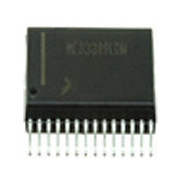
MC33889BDW Freescale, MC33889BDW Datasheet - Page 36

MC33889BDW
Manufacturer Part Number
MC33889BDW
Description
Manufacturer
Freescale
Datasheet
1.MC33889BDW.pdf
(60 pages)
Specifications of MC33889BDW
Number Of Transceivers
1
Standard Supported
CAN 2.0
Operating Supply Voltage (max)
18V
Operating Supply Voltage (min)
5.5V
Package Type
SOIC W
Supply Current
45mA
Operating Temperature (max)
125C
Operating Temperature (min)
-40C
Operating Temperature Classification
Automotive
Mounting
Surface Mount
Pin Count
28
Lead Free Status / RoHS Status
Not Compliant
Available stocks
Company
Part Number
Manufacturer
Quantity
Price
Company:
Part Number:
MC33889BDW
Manufacturer:
FREESCALE Semiconductor
Quantity:
26
Part Number:
MC33889BDW
Manufacturer:
FREESCALE
Quantity:
20 000
Table 6. Summary of RX Pin Operations for Wake up Signaling
GND SHIFT DETECTION
GENERAL
CAN transmission can afford some ground shift between
different nodes without trouble. Should a bus failure occur, the
transceiver switches to single-wire operation, therefore
working with less noise margin. The affordable ground shift is
decreased.
purpose. The four ground shift levels are selectable and the
detection is stored in the IOR register which is accessible via
the SPI.
36
33889
Table 7. 33889 Table of Operations
FUNCTIONAL DEVICE OPERATION
OPERATIONAL MODES
MODE
Notes
The following table summarizes the device behavior when a CAN Wake Up event occurs.
29.
The table below describe the SBC operation modes.
When normally working in two-wire operating mode, the
The SBC provides a ground shift detection for diagnosis
Normal Request
pulse duration is bus dominant duration minus Twake.
SBC mode
Standby
Normal
Standby
Stop
Normal
Sleep
Stop
VOLTAGE
REGULATOR
HS1 SWITCH
HS1: OFF or cyclic
HS1 controllable
HS1 controllable
(limited current
VDD1: ON
VDD1: ON
VDD1: ON
VDD1: ON
HS1: OFF
capability)
V2: OFF
V2: OFF
V2: OFF
V2: ON
CAN state
TermVbat
TermVbat
TermVbat
TermVbat
WAKE-UP
CAPABILITIES
(IF ENABLED)
CAN (always enable)
Forced Wake-up
Cyclic sense or
SPI and L0,L1
SBC mode transition to Normal
INT pulse, bit CANWU set
no event on RX, no bit set
no event on RX, no bit set
request, bit CANWU set
MC33889B
DETECTION PRINCIPLE
different values (-0.3 V, -0.7 V, -1.2 V, -1.7 V). At each TX
falling edge (end of recessive state), the CANH voltage is
sensed. If it is detected to be below the selected gnd shift
threshold, the bit SHIFT is set at 1 in the IOR register. No filter
is implemented. Required filtering for reliable detection
should be done by software (e.g. several trials).
DEVICE STATE DESCRIPTION
RESET PIN
Low for 1ms, then
Active low if W/D
Active low if W/D
Active low if W/D
or VDD1 under
or VDD1 under
or VDD1 under
Normally high.
Normally high.
Normally high.
voltage occur
voltage occur
voltage occur
The gnd shift to detect is selected via the SPI from 4
high
RX pulse (1), bit CANWU is not set
RX pulse (1), bit CANWU is not set
SBC mode transition to Normal
INT
(not maskable)
warning temp,
signal failure
signal failure
(VDD temp,
Signal SBC
CAN, HS1)
Int pulse, bit CANWU set
If enabled,
If enabled,
request, bit CANWU set
(VDD pre
wake-up
Analog Integrated Circuit Device Data
HS1)
MC33889D
SOFTWARE
WATCHDOG
- Not Running
- Running if
Freescale Semiconductor
if disabled
Running
Running
enabled
CAN CELL
Term Vbat.
Term Vbat
Term Vbat
term Vbat
Rec only
Rec only
Tx/Rx
Tx/Rx


