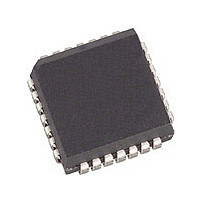
CY7B933-400JC Cypress Semiconductor Corp, CY7B933-400JC Datasheet - Page 11

CY7B933-400JC
Manufacturer Part Number
CY7B933-400JC
Description
Manufacturer
Cypress Semiconductor Corp
Datasheet
1.CY7B933-400JC.pdf
(33 pages)
Specifications of CY7B933-400JC
Lead Free Status / RoHS Status
Not Compliant
Available stocks
Company
Part Number
Manufacturer
Quantity
Price
Document #: 38-02017 Rev. *E
BIST Mode
BIST mode functions as follows:
1. Set BISTEN LOW to begin test pattern generation. Trans-
2. Set either ENA or ENN LOW to begin pattern sequence
3. Allow the Transmitter to run through several BIST loops or
START
mitter begins sending bit rate ...1010...
generation (use of the Enable pin not being used for normal
FIFO or system interface can minimize logic delays
between the controller and transmitter).
until the Receiver test is complete. RP will pulse LOW once
Tx
BEGIN
TEST
Rx
ERROR
START
TEST
LOOP
BIST
LOOP
BIST
TEST
END
Figure 6. BIST Illustration
STOP
WITHIN SPEC.
WITHIN SPEC.
Tx
DON'T CARE
DON'T CARE
DON'T CARE
DON'T CARE
DON'T CARE
HIGH
LOW
LOW
8
8
Note: It may be advisable to send violation characters to test
the RVS output in the Receiver. This can be done by explicitly
sending a violation with the SVS input, or allowing the trans-
mitter BIST loop to run while the Receiver runs in normal
mode. The BIST loop includes deliberate violation symbols
and will adequately test the RVS function.
4. When testing is completed, set BISTEN HIGH and ENA and
per BIST loop, and can be used by an external counter to
monitor the number of test pattern loops.
ENN HIGH and resume normal function.
FOTO
MODE
CKW
RP
SC/D
D
SVS
ENA
ENN
BISTEN
REFCLK
MODE
RF
CKR
SC/D
Q
RVS
RDY
BISTEN
0–7
0–7
CY7B923
CY7B933
OUTC
OUTA
OUTB
INB
INA
A/B
SO
DON'T CARE
LOW
CY7B923
CY7B933
Page 11 of 33


