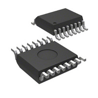
MIC2183YQS Micrel Inc, MIC2183YQS Datasheet - Page 10

MIC2183YQS
Manufacturer Part Number
MIC2183YQS
Description
QSOP-16 Low Vin Synchronous Buck PWM Control IC
Manufacturer
Micrel Inc
Datasheet
1.MIC2183YQS.pdf
(12 pages)
Specifications of MIC2183YQS
Pwm Type
Current Mode
Number Of Outputs
1
Frequency - Max
440kHz
Duty Cycle
100%
Voltage - Supply
2.9 V ~ 14 V
Buck
Yes
Boost
No
Flyback
No
Inverting
No
Doubler
No
Divider
No
Cuk
No
Isolated
No
Operating Temperature
-40°C ~ 125°C
Package / Case
16-QSOP
Frequency-max
440kHz
Lead Free Status / RoHS Status
Lead free / RoHS Compliant
Other names
576-2160
MIC2183YQS
MIC2183YQS
Available stocks
Company
Part Number
Manufacturer
Quantity
Price
Company:
Part Number:
MIC2183YQS
Manufacturer:
Micrel Inc
Quantity:
135
Part Number:
MIC2183YQS
Manufacturer:
MICREL/麦瑞
Quantity:
20 000
MIC2183
The line voltage turn on trip point is:
where:
comparator reference, typically 1.5V
The input voltage hysteresis is equal to:
where:
typically 140mV.
The MIC2183 will be disabled when the input voltage drops
back down to:
Either of 2 UVLO conditions will pull the soft start capacitor
low.
The internal bias circuit generates an internal 1.245V band-
gap reference voltage for the voltage error amplifier and a 3V
V
be decoupled with a 1µF ceramic capacitor. The capacitor
must be placed close to the V
capacitor must be connected directly to the ground plane.
MOSFET Gate Drive
The MIC2183 is designed to drive a high side P-channel
MOSFET and a low side N-channel MOSFET. The source pin
of the P-channel MOSFET is connected to the input of the
power supply. It is turned on when OUTP pulls the gate of the
MOSFET low. The advantage of using a P-channel MOSFET
is that it does not required a bootstrap circuit to boost the gate
voltage higher than the input, as would be required for an N-
channel MOSFET.
The V
drive pins, OUTN and OUTP. V
M9999-042205
DD
• When the V
• When the enable pin drops below the its enable
voltage for the internal control circuitry. The V
V
V
V
V
(V
IN
V
V
V
undervoltage lockout level.
threshold
THRESHOLD
HYST
INPUT_OFF
INPUT_ENABLE
INPUT ENABLE
INPUT HYST
INPUT_HYST
P pin (pin 16) supplies the drive voltage to both gate
THRESHOLD
R1
R2
V
IN
_
_
is the internal comparator hysteresis level,
EN/UVLO
(7)
Figure 3. UVLO Circuitry
Typical
=
1.5V
=
DD
is the voltage level of the internal
V
is the hysteresis at the input voltage
– V
=
HYST
– V
voltage drops below its
V
THRESHOLD
HYST
INPUT_HYST
Hysteresis
×
(typical)
140mV
R
)
1
×
R
MIC2183
DD
+
R
IN
2
R
1
R
P pin is usually connected
×
+
2
pin. The other end of the
2
R
R
Circuitry
=
1
2
Bias
R
+
2
R
2
DD
pin must
10
to the input supply. The V
connected to the same potential.
A non-overlap time is built into the MOSFET driver circuitry.
This dead-time prevents the high-side and low-side MOSFET
drivers from being on at the same time. Either an external
diode or the low-side MOSFET internal parasitic diode con-
ducts the inductor current during the dead-time.
MOSFET Selection
The P-channel MOSFET must have a V
equal to or lower than the input voltage when used in a buck
converter topology. There is a limit to the maximum gate
charge the MIC2183 will drive. Higher gate charge MOSFETs
will slow down the turn-on and turn-off times of the MOSFETs.
Slower transition times will cause higher power dissipation in
the MOSFETs due to higher switching transition losses. The
MOSFETs must be able to completely turn on and off within
the driver non-overlap time If both MOSFETs are conducting
at the same time, shoot-through will occur, which greatly
increases power dissipation in the MOSFETs and reduces
converter efficiency.
The MOSFET gate charge is also limited by power dissipation
in the MIC2183. The power dissipated by the gate drive
circuitry is calculated below:
where: Qgate is the total gate charge of both the N and P-
channel MOSFETs.
The graph in Figure 4 shows the total gate charge that can be
driven by the MIC2183 over the input voltage range, for
different values of switching frequency.
Oscillator & Sync
The internal oscillator is free running and requires no external
components. The f/2 pin allows the user to select from two
switching frequencies. A low level set the oscillator frequency
to 400kHz and a high level set the oscillator frequency to
200kHz. The maximum duty cycle for both frequencies is
100%. This is another advantage of using a P-channel
MOSFET for the high-side drive; it can continuously turned
on.
A frequency foldback mode is enabled if the voltage on the
feedback pin (pin 6) is less than 0.3V. In frequency foldback,
Figure 4. MIC2183 Frequency vs Max. Gate Charge
P
f
V
S
GATE_DRIVE
IN
is the switching frequency
P is the gate drive voltage at the V
140
130
120
110
100
90
80
70
60
50
40
=
3
Q
500kHz
5
GATE
Max. Gate Charge
INPUT VOLTAGE (V)
Frequency vs.
7
IN
×
P pin and CSH pin must be
600kHz
V P f
9
IN
11
×
S
300kHz
400kHz
200kH
13
GS
15
threshold voltage
IN
P pin
Micrel, Inc.
April 2005


