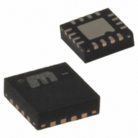
MIC2215-PPGBML TR Micrel Inc, MIC2215-PPGBML TR Datasheet - Page 9

MIC2215-PPGBML TR
Manufacturer Part Number
MIC2215-PPGBML TR
Description
Triple Low Noise High PSRR Cap LDO
Manufacturer
Micrel Inc
Datasheet
1.MIC2215-PPMYML_TR.pdf
(11 pages)
Specifications of MIC2215-PPGBML TR
Regulator Topology
Positive Fixed
Voltage - Output
3V, 3V, 1.8V
Voltage - Input
2.25 ~ 5.5 V
Voltage - Dropout (typical)
0.17V @ 250mA
Number Of Regulators
3
Current - Output
250mA
Current - Limit (min)
350mA
Operating Temperature
-40°C ~ 125°C
Mounting Type
Surface Mount
Package / Case
16-MLF®, QFN
Lead Free Status / RoHS Status
Contains lead / RoHS non-compliant
Other names
MIC2215-PPGBMLTR
MIC2215-PPGBMLTR
MIC2215-PPGBMLTR
Application Information
Enable/Shutdown
The MIC2215 comes with three active-high enable pins
that allow control of each individual regulator to be either
disabled or enabled. Forcing the enable pin low disables
the respective regulator and sends it into a “zero” off-
mode-current state. In this state, current consumed by
the individual regulator goes nearly to zero. This is true
for both regulators 2 and 3. Regulator 1’s input supply
pin is also used to power the internal reference. When
any regulator; either 1, 2, or 3 is enabled, an additional
20µA for the reference will be drawn through V
three must be disabled to enter the “zero” current-off-
mode-state. Forcing the enable pin high enables each
respective output voltage. This part is CMOS and none
of the enable pins can be left floating; a floating enable
pin may cause an indeterminate state on the output.
Input Capacitor
The MIC2215 is a high performance, high bandwidth
device. Therefore, it requires a well-bypassed input
supply for optimal performance. A small 0.1µF capacitor
placed close to the input is recommended to aid in noise
performance. Low-ESR ceramic capacitors provide opti-
mal performance at a mini-mum of space. Additional
high-frequency capacitors such as small valued NPO
dielectric type capacitors help to filter out high frequency
noise and are good practice in any RF-based circuit.
Output Capacitor
The MIC2215 requires an output capacitor for stability.
The design requires 1µF or greater on the output to
maintain stability. The design is optimized for use with
low-ESR ceramic chip capacitors. X7R/X5R dielectric-
type ceramic capacitors are recommended because of
their temperature performance. X7R-type capacitors
change capacitance by 15% over their operating temp-
erature range and are the most stable type of ceramic
capacitors. Z5U and Y5V dielectric capacitors change
value by as much as 50% and 60%, respectively, over
their operating temperature ranges. To use a ceramic
chip capacitor with Y5V dielectric, the value must be
much higher than an X7R ceramic capacitor to ensure
the same minimum capacitance over the equivalent
operating temperature range.
Bypass Pin
A capacitor can be placed from the noise bypass pin to
ground to reduce output voltage noise. The capacitor
bypasses the internal reference. There is one single
internal reference shared by each output, therefore the
bypassing affects each regulator. A 0.1µF capacitor is
recommended for applications that require low-noise
outputs. The bypass capacitor can be increased, further
reducing noise and improving PSRR. Turn-on time
increases slightly with respect to bypass capacitance.
Micrel, Inc.
January 2007
IN1
. All
9
Internal Reference
The internal band gap, or reference, is powered from the
V
contributions being imposed on the band gap, it is
important to make V
bypassing close to the input.
Multiple Input Supplies
The MIC2215 can be used with multiple input supplies
when desired. The only requirement, aside from
maintaining the voltages within the operating ranges, is
that V
No-Load Stability
The MIC2215 will remain stable and in regulation with no
load, unlike many other voltage regulators. This is
especially important in CMOS RAM keep-alive app-
lications.
Thermal Considerations
The MIC2215 is designed to provide up to 250mA of
current per channel in a very small package. Maximum
power dissipation can be calculated based on the output
current and the voltage drop across the part. To
determine the maximum power dissipation of the
package, use the junction-to-ambient thermal resistance
of the device and the following basic equation:
T
125°C, and T
is layout dependent; Table 2 shows examples of the
junction-to-ambient thermal resistance for the MIC2215.
The actual power dissipation of the regulator circuit can
be determined using the equation:
Substituting P
conditions that are critical to the application will give the
maximum operating conditions for the regulator circuit.
For example, when operating the MIC2215 at 60°C with
a minimum footprint layout, the maximum load currents
can be calculated as follows:
J(max)
IN1
16-Pin 4mm x 4mm MLF
input. Due to some of the input noise (PSRR)
IN1
is the maximum junction temperature of the die,
P
P
P
P
P
P
P
always remains the highest voltage potential.
Package
D(max)
DTOTAL
DLDO1
DLDO2
DLDO3
D (max)
D (max)
Table 2. MLF
A
D (max)
= (T
= (V
= (V
= (V
is the ambient operating temperature. θ
= (125°C – 60°C)/43 °C/W
= 1.511W
= P
J(max)
IN1
IN2
IN3
DLDO1
for P
IN1
– V
– V
– V
®
– T
®
as clean as possible with good
+ P
D
OUT1
OUT2
OUT3
Thermal Resistance
and solving for the operating
A
)÷θ
DLDO2
) × I
) × I
) × I
JA
Minimum Footprint
OUT1
OUT2
OUT3
θ
+ P
JA
Recommended
DLDO3
43°C/W
M9999-011207
MIC2215
JA


