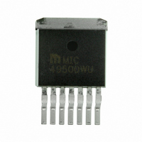
MIC49500WU Micrel Inc, MIC49500WU Datasheet - Page 8

MIC49500WU
Manufacturer Part Number
MIC49500WU
Description
5A LDO, Low Vin, Low Vout, Fast Transient Response, Cap Stable ( )
Manufacturer
Micrel Inc
Datasheet
1.MIC49500WR_TR.pdf
(11 pages)
Specifications of MIC49500WU
Regulator Topology
Positive Adjustable
Voltage - Output
0.7 ~ 6 V
Voltage - Input
1.4 ~ 6 V
Voltage - Dropout (typical)
0.29V @ 5A
Number Of Regulators
1
Current - Output
5A
Current - Limit (min)
5.5A
Operating Temperature
-40°C ~ 125°C
Mounting Type
Surface Mount
Package / Case
TO-263-7, D²Pak (7 leads + Tab), TO-263CA
Lead Free Status / RoHS Status
Lead free / RoHS Compliant
Other names
576-2350
MIC49500WU
MIC49500WU
July 2007
Applications Information
The MIC49500 is an ultra-high performance, low
dropout linear regulator designed for high current
applications requiring fast transient response. The
MIC49500 utilizes two input supplies, significantly
reducing dropout voltage, perfect for low-voltage, DC-
to-DC conversion. The MIC49500 requires a minimum
of external components and obtains a bandwidth of up
to 10MHz. As a µCap regulator, the output is tolerant
of virtually any type of capacitor including ceramic and
tantalum.
The MIC49500 regulator is fully protected from
damage due to fault conditions, offering constant
current limiting and thermal shutdown.
Bias Supply Voltage
V
to the control portion of the MIC49500. V
approximately 70mA for 5A load current. Most of the
biasing current is used to supply the base current to
the pass transistor. This allows the pass element to be
driven into saturation, reducing the dropout to 290mV
at a 5A load current. Bypassing on the bias pin is
recommended
regulator during line and load transients. Small
ceramic capacitors from V
high frequency noise from being injected into the
control circuitry from the bias rail and are good design
practice. Good bypass techniques typically include
one larger capacitor such as 1µF ceramic and smaller
valued capacitors such as 0.01µF or 0.001µF in
parallel with that larger capacitor to decouple the bias
supply. The V
the output voltage with a minimum V
of 3.0V.
Input Supply Voltage
V
pass transistor. The minimum input voltage is 1.4V,
allowing conversion from low voltage supplies.
Output Capacitor
The MIC49500 requires a minimum of output
capacitance to maintain stability. However, proper
capacitor selection is important to ensure desired
transient response. The MIC49500 is specifically
designed to be stable with a wide range of
capacitance values and ESR. A 10µF ceramic chip
capacitor should satisfy most applications. Output
capacitance can be increased without bound. See
typical characteristics for examples of load transient
response.
X7R dielectric ceramic capacitors are recommended
because of their temperature performance. X7R-type
BIAS
IN
provides the high current to the collector of the
, requiring relatively light current, provides power
BIAS
to
input voltage must be 2.1V above
improve
BIAS
to ground help reduce
performance
BIAS
input voltage
BIAS
requires
of
the
8
capacitors change capacitance by 15% over their
operating temperature range and are the most stable
type of ceramic capacitors. Z5U and Y5V dielectric
capacitors change value by as much as 50% and
60%, respectively, over their operating temperature
ranges. To use a ceramic chip capacitor with Y5V
dielectric, the value must be much higher than an X7R
ceramic or a tantalum capacitor to ensure the same
capacitance value over the operating temperature
range. Tantalum capacitors have a very stable
dielectric (10% over their operating temperature
range) and can also be used with this device.
Input Capacitor
An input capacitor of 1µF or greater is recommended
when the device is more than 4 inches away from the
bulk supply capacitance, or when the supply is a
battery. Small, surface mount, ceramic chip capacitors
can be used for the bypassing. The capacitor should
be placed within 1" of the device for optimal
performance. Larger values will help to improve ripple
rejection by bypassing the input to the regulator,
further improving the integrity of the output voltage.
Thermal Design
Linear regulators are simple to use. The most
complicated design parameters to consider are
thermal characteristics. Thermal design requires the
following application-specific parameters:
First, calculate the power dissipation of the regulator
from these numbers and the device parameters from
this datasheet.
The input current will be less than the output current
as the output load increases. The bias current is a
sum of base drive and ground current. Ground current
is constant over load current. Then the heat sink
thermal resistance is determined with this formula:
The heat sink may be significantly reduced in
applications where the maximum input voltage is
known and large compared with the dropout voltage.
Use a series input resistor to drop excessive voltage
and distribute the heat between this resistor and the
•
•
•
•
•
Maximum ambient temperature (T
Output Current (I
Output Voltage (V
Input Voltage (V
Ground Current (I
P
SA
D
= V
=
⎛
⎝
IN
P
× I
D
T
J(MAX)
IN
+ V
JC
IN
BIAS
OUT
)
± T
GND
OUT
)
)
)
CS
A
× I
)
BIAS
– V
OUT
M9999-071307
A
× I
)
OUT


