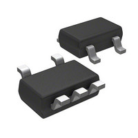
MIC922YC5 TR Micrel Inc, MIC922YC5 TR Datasheet - Page 10

MIC922YC5 TR
Manufacturer Part Number
MIC922YC5 TR
Description
Op Amp, 1500V/us, 230MHz GBW, 2.5mA, SC70 ( )
Manufacturer
Micrel Inc
Series
Teeny™r
Datasheet
1.MIC922YC5_TR.pdf
(11 pages)
Specifications of MIC922YC5 TR
Amplifier Type
General Purpose
Number Of Circuits
1
Slew Rate
1500 V/µs
Gain Bandwidth Product
230MHz
-3db Bandwidth
400MHz
Current - Input Bias
1.7µA
Voltage - Input Offset
400µV
Current - Supply
2.5mA
Current - Output / Channel
84mA
Voltage - Supply, Single/dual (±)
±2.5 V ~ 9 V
Operating Temperature
-40°C ~ 85°C
Mounting Type
Surface Mount
Package / Case
SC-70-5, SC-88A, SOT-323-5, SOT-353, 5-TSSOP
Lead Free Status / RoHS Status
Lead free / RoHS Compliant
Output Type
-
Lead Free Status / RoHS Status
Lead free / RoHS Compliant
Other names
MIC922YC5TR
MIC922YC5TR
MIC922YC5TR
MIC922
Applications Information
The MIC922 is a high-speed, voltage-feedback operational
amplifier featuring very low supply current and excellent
stability. This device is unity gain stable, capable of driving
high capacitance loads.
Driving High Capacitance
The MIC922 is stable when driving high capacitance, making
it ideal for driving long coaxial cables or other high-capaci-
tance loads. Most high-speed op amps are only able to drive
limited capacitance.
Feedback Resistor/Capacitor Selection
Conventional op amp gain configurations and resistor selec-
tion apply, the MIC922 is NOT a current feedback device.
Also, for minimum peaking, the feedback resistor should
have low parasitic capacitance. To use the part as a follower,
the output should be connected to input via a short wire. At
high frequency, the parasitic capacitance at the input might
cause peaking in the closed-loop frequency response. A
1pF capacitor should be used across the feedback resistor
to compensate for this parasitic peaking.
Layout Considerations
All high speed devices require careful PCB layout. The follow-
ing guidelines should be observed: Capacitance, par-ticularly
on the two inputs pins will degrade performance; avoid large
copper traces to the inputs. Keep the output signal away from
the inputs and use a ground plane.
MIC922
Note: increasing load capacitance does reduce
the speed of the device. In applications where
the load capacitance reduces the speed of the
op amp to an unacceptable level, the effect of
the load capacitance can be reduced by add-
ing a small resistor (<100Ω) in series with the
output.
10
It is important to ensure adequate supply bypassing capaci-
tors are located close to the device.
Power Supply Bypassing
Regular supply bypassing techniques are recommended.
A 10µF capacitor in parallel with a 0.1µF capacitor on both
the positive and negative supplies are ideal. For best perfor-
mance all bypassing capacitors should be located as close
to the op amp as possible and all capacitors should be low
ESL (equivalent series inductance), ESR (equivalent series
resis-tance). Surface-mount ceramic capacitors are ideal.
Thermal Considerations
The SC70-5 package, like all small packages, has a high
thermal resistance. It is important to ensure the IC does not
exceed the maximum operating junction (die) temperature of
85°C. The part can be operated up to the absolute maximum
temperature rating of 125°C, but between 85°C and 125°C
performance will degrade, in par-ticular CMRR will reduce.
An MIC922 with no load, dissipates power equal to the qui-
escent supply current × supply voltage
When a load is added, the additional power is dissipated in
the output stage of the op amp. The power dissipated in the
device is a function of supply voltage, output voltage and
output current.
Ensure the total power dissipated in the device is no greater
than the thermal capacity of the package. The SC70-5 pack-
age has a thermal resistance of 450°C/W.
P
P
Total Power Dissipation = P
Max. Allowable Power Dissipation =
D(no load)
D(output stage)
= (V
= (V
V+
– V
V+
V-
– V
)I
S
VOUT
D(no load)
)I
OUT
+ P
T
J(max)
D(output stage)
450°C/W
Micrel, Inc.
May 2006
– T
A(max)


