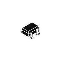
NCP4682DSQ25T1G ON Semiconductor, NCP4682DSQ25T1G Datasheet - Page 18

NCP4682DSQ25T1G
Manufacturer Part Number
NCP4682DSQ25T1G
Description
150MA LDO REGULATOR
Manufacturer
ON Semiconductor
Series
-r
Datasheet
1.NCP4682DMU15TCG.pdf
(22 pages)
Specifications of NCP4682DSQ25T1G
Regulator Topology
Positive Fixed
Voltage - Output
2.5V
Voltage - Input
Up to 5.25V
Voltage - Dropout (typical)
0.28V @ 150mA
Number Of Regulators
1
Current - Output
150mA (Min)
Current - Limit (min)
-
Operating Temperature
-40°C ~ 85°C
Mounting Type
Surface Mount
Package / Case
SC-82
Number Of Outputs
1
Input Voltage Max
6 V
Output Voltage
2.5 V
Dropout Voltage (max)
0.24 V
Output Current
150 mA
Load Regulation
20 mV
Voltage Regulation Accuracy
0.8 %
Maximum Power Dissipation
380 mW
Mounting Style
SMD/SMT
Lead Free Status / Rohs Status
Lead free / RoHS Compliant
Available stocks
Company
Part Number
Manufacturer
Quantity
Price
Company:
Part Number:
NCP4682DSQ25T1G
Manufacturer:
ON Semiconductor
Quantity:
2 350
series is shown in Figure 58.
Input Decoupling Capacitor (C1)
connected as close as possible to the input and ground pin of
the NCP4682/5. Higher values and lower ESR improves line
transient response.
Output Decoupling Capacitor (C2)
to achieve stable operation of the IC. If a tantalum capacitor
is used, and its ESR is high, loop oscillation may result. The
capacitors should be connected as close as possible to the
output and ground pins. Larger values and lower ESR
improves dynamic parameters.
Current Limit
circuit. This type of protection doesn’t limit output current
A typical application circuits for NCP4682 and NCP4685
A 0.1 mF ceramic input decoupling capacitor should be
A 0.1 mF ceramic output decoupling capacitor is enough
This regulator includes a fold−back current limiting
VIN
VIN
100n
Figure 58. Typical Application Schematic
100n
C1
C1
VIN
CE
VIN
NCP4682x
NCP4685x
GND
GND
VOUT
VOUT
APPLICATION INFORMATION
C2
100n
C2
100n
VOUT
VOUT
http://onsemi.com
18
up to specified current capability in normal operation, but
when an over current situation occurs, the output voltage and
current decrease until the over current condition ends.
Typical characteristics of this protection scheme are shown
in the Output voltage versus Output current graphs in the
characterization section of this datasheet.
Enable Operation (NCP4682 Only)
on and off. The IC is switched on when a high level voltage
is applied to the CE pin. The enable pin has an internal pull
down current source. If the enable function is not needed,
connect CE pin to VIN.
Output Discharger (NCP4682 Only)
VOUT and GND that is used for faster discharging of the
output capacitor. This function is activated when the IC goes
into disable mode.
Thermals
necessary to provide some thermal relief. The maximum
power dissipation supported by the device is dependent
upon board design and layout. Mounting pad configuration
on the PCB, the board material, and also the ambient
temperature affect the rate of temperature increase for the
part. When the device has good thermal conductivity
through the PCB the junction temperature will be relatively
low in high power dissipation applications.
PCB layout
impedance is high, noise pickup or unstable operation may
result. Connect capacitors C1 and C2 as close as possible to
the IC, and make wiring as short as possible.
The enable pin CE may be used for turning the regulator
The NCP4682D version includes a transistor between
As a power across the IC increase, it might become
Make the VIN and GND line as large as practical. If their


