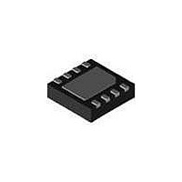
PIC12LF1840-E/MF Microchip Technology, PIC12LF1840-E/MF Datasheet - Page 103

PIC12LF1840-E/MF
Manufacturer Part Number
PIC12LF1840-E/MF
Description
7 KB Flash, 256 Bytes RAM, 32 MHz Int. Osc, 6 I/0, Enhanced Mid Range Core, Nano
Manufacturer
Microchip Technology
Series
PIC® XLP™ 12Fr
Datasheet
1.PIC12F1840-EMF.pdf
(382 pages)
Specifications of PIC12LF1840-E/MF
Processor Series
PIC12F
Core
PIC
Program Memory Type
Flash
Program Memory Size
7 KB
Data Ram Size
256 B
Interface Type
MI2C, SPI, EUSART
Number Of Timers
3
Operating Supply Voltage
1.8 V to 5.5 V
Maximum Operating Temperature
+ 125 C
Mounting Style
SMD/SMT
Package / Case
DFN-8
Development Tools By Supplier
MPLAB IDE Software
Minimum Operating Temperature
- 40 C
Core Processor
RISC
Core Size
8-Bit
Speed
32MHz
Connectivity
I²C, LIN, SPI, UART/USART
Peripherals
Brown-out Detect/Reset, POR, PWM, WDT
Number Of I /o
5
Eeprom Size
256 x 8
Ram Size
256 x 8
Voltage - Supply (vcc/vdd)
1.8 V ~ 3.6 V
Data Converters
A/D 4x10b
Oscillator Type
Internal
Operating Temperature
-40°C ~ 125°C
Lead Free Status / Rohs Status
Details
Available stocks
Company
Part Number
Manufacturer
Quantity
Price
Company:
Part Number:
PIC12LF1840-E/MF
Manufacturer:
MICROCHIP
Quantity:
12 000
- Current page: 103 of 382
- Download datasheet (4Mb)
After the “BSF EECON1,WR” instruction, the processor
requires two cycles to set up the write operation. The
user must place two NOP instructions after the WR bit is
set. The processor will halt internal operations for the
typical 2 ms, only during the cycle in which the write
takes place (i.e., the last word of the block write). This
is not Sleep mode as the clocks and peripherals will
FIGURE 11-2:
2011 Microchip Technology Inc.
EEADRL<4:0> = 00000
First word of block
to be written
Buffer Register
BLOCK WRITES TO FLASH PROGRAM MEMORY WITH 32 WRITE LATCHES
14
EEADRL<4:0> = 00001
7
Buffer Register
5
EEDATH
Preliminary
6
14
Program Memory
EEADRL<4:0> = 00010
0 7
continue to run. The processor does not stall when
LWLO = 1, loading the write latches. After the write
cycle, the processor will resume operation with the third
instruction after the EECON1 write instruction.
EEDATA
Buffer Register
8
14
PIC12(L)F1840
EEADRL<4:0> = 11111
0
Buffer Register
Last word of block
DS41441B-page 103
to be written
14
Related parts for PIC12LF1840-E/MF
Image
Part Number
Description
Manufacturer
Datasheet
Request
R

Part Number:
Description:
Manufacturer:
Microchip Technology Inc.
Datasheet:

Part Number:
Description:
Manufacturer:
Microchip Technology Inc.
Datasheet:

Part Number:
Description:
Manufacturer:
Microchip Technology Inc.
Datasheet:

Part Number:
Description:
Manufacturer:
Microchip Technology Inc.
Datasheet:

Part Number:
Description:
Manufacturer:
Microchip Technology Inc.
Datasheet:

Part Number:
Description:
Manufacturer:
Microchip Technology Inc.
Datasheet:

Part Number:
Description:
Manufacturer:
Microchip Technology Inc.
Datasheet:

Part Number:
Description:
Manufacturer:
Microchip Technology Inc.
Datasheet:


