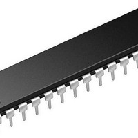
PIC16F1518-E/SP Microchip Technology, PIC16F1518-E/SP Datasheet - Page 122

PIC16F1518-E/SP
Manufacturer Part Number
PIC16F1518-E/SP
Description
28-pin, 28KB Flash, 1024B RAM, 10-bit ADC, 2xCCP, SPI, MI2C, EUSART, 2.3V-5.5V 2
Manufacturer
Microchip Technology
Series
PIC® XLP™ 16Fr
Datasheet
1.PIC16F1516-EMV.pdf
(344 pages)
Specifications of PIC16F1518-E/SP
Processor Series
PIC16F151x
Core
PIC
Data Bus Width
8 bit
Program Memory Type
Flash
Program Memory Size
16 KB
Data Ram Size
1 KB
Interface Type
I2C, SPI, USART
Maximum Clock Frequency
20 MHz
Number Of Programmable I/os
25
Number Of Timers
3
Operating Supply Voltage
2.3 V to 5.5 V
Maximum Operating Temperature
+ 125 C
Mounting Style
Through Hole
Package / Case
PDIP-28
Core Processor
PIC
Core Size
8-Bit
Speed
20MHz
Connectivity
I²C, LIN, SPI, UART/USART
Peripherals
Brown-out Detect/Reset, POR, PWM, WDT
Number Of I /o
25
Eeprom Size
-
Ram Size
1K x 8
Voltage - Supply (vcc/vdd)
2.3 V ~ 5.5 V
Data Converters
A/D 17x10b
Oscillator Type
Internal
Operating Temperature
-40°C ~ 125°C
Lead Free Status / Rohs Status
Details
- Current page: 122 of 344
- Download datasheet (3Mb)
PIC16(L)F1516/7/8/9
12.4
PORTC is a 8-bit wide bidirectional port. The
corresponding
(Register
corresponding PORTC pin an input (i.e., put the
corresponding output driver in a High-Impedance mode).
Clearing a TRISC bit (= 0) will make the corresponding
PORTC pin an output (i.e., enable the output driver and
put the contents of the output latch on the selected pin).
Example 12-1
Reading the PORTC register
status of the pins, whereas writing to it will write to the
PORT latch. All write operations are read-modify-write
operations. Therefore, a write to a port implies that the
port pins are read, this value is modified and then written
to the PORT data latch (LATC).
The TRISC register
PORTC pin output drivers, even when they are being
used as analog inputs. The user should ensure the bits in
the TRISC register are maintained set when using them
as analog inputs. I/O pins configured as analog input
always read ‘0’.
12.4.1
The ANSELC register
configure the Input mode of an I/O pin to analog.
Setting the appropriate ANSELC bit high will cause all
digital reads on the pin to be read as ‘0’ and allow
analog functions on the pin to operate correctly.
The state of the ANSELC bits has no affect on digital out-
put functions. A pin with TRIS clear and ANSELC set will
still operate as a digital output, but the Input mode will be
analog. This can cause unexpected behavior when exe-
cuting read-modify-write instructions on the affected
port.
DS41452B-page 122
Note:
PORTC Registers
12-12). Setting a TRISC bit (= 1) will make the
ANSELC REGISTER
The ANSELC register must be initialized
to configure an analog channel as a digital
input. Pins configured as analog inputs
will read ‘0’.
shows how to initialize an I/O port.
data
direction
(Register
(Register
(Register
12-12) controls the
register
12-14) is used to
12-11) reads the
is
TRISC
Preliminary
12.4.2
Each PORTC pin is multiplexed with other functions. The
pins, their combined functions and their output priorities
are shown in
When multiple outputs are enabled, the actual pin
control goes to the peripheral with the highest priority.
Analog input and some digital input functions are not
included in the list below. These input functions can
remain active when the pin is configured as an output.
Certain digital input functions override other port
functions and are included in
TABLE 12-7:
Note 1:
Pin Name
2:
RC0
RC1
RC2
RC3
RC4
RC5
RC6
RC7
Priority listed from highest to lowest.
RC3 and RC4 read the I
I
PORTC FUNCTIONS AND OUTPUT
PRIORITIES
2
Table
C mode is enabled.
PORTC OUTPUT PRIORITY
12-7.
2010 Microchip Technology Inc.
Function Priority
Table
SOSCO
RC0
SOSCI
CCP2
RC1
CCP1
RC2
SCL
SCK
RC3
SDA
RC4
SDO
RC5
CK
TX
RC6
DT
RC7
12-7.
2
C ST input when
(2)
(2)
(1)
Related parts for PIC16F1518-E/SP
Image
Part Number
Description
Manufacturer
Datasheet
Request
R

Part Number:
Description:
IC, 8BIT MCU, PIC16F, 32MHZ, SOIC-18
Manufacturer:
Microchip Technology
Datasheet:

Part Number:
Description:
IC, 8BIT MCU, PIC16F, 32MHZ, SSOP-20
Manufacturer:
Microchip Technology
Datasheet:

Part Number:
Description:
IC, 8BIT MCU, PIC16F, 32MHZ, DIP-18
Manufacturer:
Microchip Technology
Datasheet:

Part Number:
Description:
IC, 8BIT MCU, PIC16F, 32MHZ, QFN-28
Manufacturer:
Microchip Technology
Datasheet:

Part Number:
Description:
IC, 8BIT MCU, PIC16F, 32MHZ, QFN-28
Manufacturer:
Microchip Technology
Datasheet:

Part Number:
Description:
IC, 8BIT MCU, PIC16F, 32MHZ, QFN-28
Manufacturer:
Microchip Technology
Datasheet:

Part Number:
Description:
IC, 8BIT MCU, PIC16F, 32MHZ, SSOP-20
Manufacturer:
Microchip Technology
Datasheet:

Part Number:
Description:
IC, 8BIT MCU, PIC16F, 20MHZ, DIP-40
Manufacturer:
Microchip Technology
Datasheet:

Part Number:
Description:
IC, 8BIT MCU, PIC16F, 32MHZ, QFN-28
Manufacturer:
Microchip Technology
Datasheet:

Part Number:
Description:
IC, 8BIT MCU, PIC16F, 20MHZ, MQFP-44
Manufacturer:
Microchip Technology
Datasheet:

Part Number:
Description:
IC, 8BIT MCU, PIC16F, 20MHZ, QFN-20
Manufacturer:
Microchip Technology
Datasheet:

Part Number:
Description:
IC, 8BIT MCU, PIC16F, 32MHZ, QFN-28
Manufacturer:
Microchip Technology
Datasheet:

Part Number:
Description:
MCU 14KB FLASH 768B RAM 64-TQFP
Manufacturer:
Microchip Technology
Datasheet:

Part Number:
Description:
7 KB Flash, 384 Bytes RAM, 32 MHz Int. Osc, 16 I/0, Enhanced Mid Range Core, Low
Manufacturer:
Microchip Technology

Part Number:
Description:
14KB Flash, 512B RAM, 256B EEPROM, LCD, 1.8-5.5V 40 UQFN 5x5x0.5mm TUBE
Manufacturer:
Microchip Technology
Datasheet:


