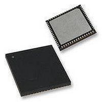
PIC16F1947-E/MR Microchip Technology, PIC16F1947-E/MR Datasheet - Page 4

PIC16F1947-E/MR
Manufacturer Part Number
PIC16F1947-E/MR
Description
28KB Flash, 1KB RAM, 256B EEPROM, LCD, 1.8-5.5V 64 QFN 9x9x0.9mm TUBE
Manufacturer
Microchip Technology
Series
PIC® XLP™ 16Fr
Datasheets
1.PIC16F722-ISS.pdf
(8 pages)
2.PIC16LF1933-ISS.pdf
(46 pages)
3.PIC16LF1946-IPT.pdf
(448 pages)
4.PIC16LF1946-IPT.pdf
(6 pages)
5.PIC16F1946-IPT.pdf
(8 pages)
Specifications of PIC16F1947-E/MR
Core Processor
PIC
Core Size
8-Bit
Speed
32MHz
Connectivity
I²C, LIN, SPI, UART/USART
Peripherals
Brown-out Detect/Reset, LCD, POR, PWM, WDT
Number Of I /o
54
Program Memory Size
28KB (16K x 14)
Program Memory Type
FLASH
Eeprom Size
256 x 8
Ram Size
1K x 8
Voltage - Supply (vcc/vdd)
1.8 V ~ 5.5 V
Data Converters
A/D 17x10b
Oscillator Type
Internal
Operating Temperature
-40°C ~ 125°C
Package / Case
64-VQFN Exposed Pad, 64-HVQFN, 64-SQFN, 64-DHVQFN
Processor Series
PIC16F
Core
PIC
Data Bus Width
8 bit
Data Ram Size
1 KB
Interface Type
MI2C, SPI, EUSART
Maximum Clock Frequency
32 MHz
Number Of Programmable I/os
54
Number Of Timers
5
Operating Supply Voltage
1.8 V to 5.5 V
Maximum Operating Temperature
+ 125 C
Mounting Style
SMD/SMT
3rd Party Development Tools
52715-96, 52716-328, 52717-734
Development Tools By Supplier
PG164130, DV164035, DV244005, DV164005
Minimum Operating Temperature
- 40 C
On-chip Adc
10 bit, 17 Channel
On-chip Dac
5 bit
Lead Free Status / RoHS Status
Lead free / RoHS Compliant
Lead Free Status / RoHS Status
Lead free / RoHS Compliant
PIC16(L)F1946/1947
EXAMPLE 1:
For other combinations of F
Instruction cycle delay counts, refer to
TABLE 3:
DS80497C-page 4
BSF
BCF
MOVF
Note:
32 MHz
16 MHz
8 MHz
In
required to complete the full conversion. Each T
cycle consists of 8 T
provided to stop the A/D conversion after 86
instruction cycles and terminate the conversion at
the correct time as shown in the figure above.
Affected Silicon Revisions
F
OSC
A2
X
Figure
ADCON0, ADGO
ADCON0, ADGO
ADRESH, W
The exact delay time will depend on the
choice of F
(ADCS) selection. The T
in the timing diagram above apply to this
example only. Refer to
required
configurations.
A3
1, 88 instruction cycles (T
INSTRUCTION CYCLE DELAY
COUNTS FOR OTHER F
AND T
F
F
F
F
F
F
F
OSC
OSC
OSC
OSC
OSC
OSC
OSC
A4
T
CODE EXAMPLE OF
INSTRUCTION CYCLE
DELAY
AD
/64
/32
/64
/32
/16
/32
/16
delay
AD
OSC
CY
; Start ADC conversion
; Provide 86
; Terminate the
; Read conversion
COMBINATIONS
Instruction Cycle Delay
instruction cycle
delay here
conversion manually
result
periods. A fixed delay is
and the T
OSC
counts
, T
CY
Counts
Table 3
AD
Table
172
172
counts shown
86
86
43
86
43
for
AD
values and
CY
3.
OSC
) will be
for the
divisor
other
AD
3. Module: Brown-out Reset (BOR)
3.1 Brown-out Reset
4. Module: Enhanced Capture Compare
4.1 Enhanced PWM
4.2 Enhanced PWM
If MCLR is used to wake the device, while the BOR
is set to Sleep and the part is in Sleep, the BOR bit
of the PCON register will be cleared without V
dropping below the BOR level.
Work around
None.
Affected Silicon Revisions
When the PWM is configured for Full-Bridge mode
and the duty cycle is set to 0%, writing the
PxM<1:0> bits to change the direction has no
effect on PxA and PxC outputs.
Work around
Increase the duty cycle to a value greater than 0%
before changing directions.
Affected Silicon Revisions
In PWM mode, when the duty cycle is set to 0%
and the STRxSYNC bit is set, writing the STRxA,
STRxB, STRxC and the STRxD bits to enable/
disable steering to port pins has no effect on the
outputs.
Work around
Increase the duty cycle to a value greater than 0%
before enabling/disabling steering to port pins.
Affected Silicon Revisions
A2
A2
A2
X
X
X
A3
A3
A3
X
PWM (ECCP)
A4
A4
A4
X
2010 Microchip Technology Inc.
DD


