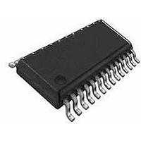
PIC16LF1903-E/SS Microchip Technology, PIC16LF1903-E/SS Datasheet - Page 135

PIC16LF1903-E/SS
Manufacturer Part Number
PIC16LF1903-E/SS
Description
7KB Flash, 256B RAM, LCD, 11x10b ADC, NanoWatt XLP 28 SSOP .209in TUBE
Manufacturer
Microchip Technology
Series
PIC® XLP™ 16Fr
Datasheet
1.PIC16LF1902-EMV.pdf
(240 pages)
Specifications of PIC16LF1903-E/SS
Processor Series
PIC16LF190x
Core
PIC
Data Bus Width
8 bit
Program Memory Type
Flash
Program Memory Size
4 KB
Data Ram Size
256 B
Maximum Clock Frequency
20 MHz
Number Of Programmable I/os
25
Number Of Timers
2
Operating Supply Voltage
1.8 V to 3.6 V
Maximum Operating Temperature
+ 125 C
Mounting Style
SMD/SMT
Package / Case
SSOP-28
Core Processor
PIC
Core Size
8-Bit
Speed
20MHz
Connectivity
-
Peripherals
Brown-out Detect/Reset, LCD, POR, PWM, WDT
Number Of I /o
25
Eeprom Size
-
Ram Size
256 x 8
Voltage - Supply (vcc/vdd)
1.8 V ~ 3.6 V
Data Converters
A/D 11x10b
Oscillator Type
Internal
Operating Temperature
-40°C ~ 125°C
Lead Free Status / Rohs Status
Details
- Current page: 135 of 240
- Download datasheet (3Mb)
17.3
Timer1 has four prescaler options allowing 1, 2, 4 or 8
divisions of the clock input. The T1CKPS bits of the
T1CON register control the prescale counter. The
prescale counter is not directly readable or writable;
however, the prescaler counter is cleared upon a write to
TMR1H or TMR1L.
17.4
A dedicated low-power 32.768 kHz oscillator circuit is
built-in between pins T1OSI (input) and T1OSO. This
internal circuit is to be used in conjunction with an
external 32.768 kHz crystal.
The oscillator circuit is enabled by setting the
T1OSCEN bit of the T1CON register. The oscillator will
continue to run during Sleep.
17.5
If control bit T1SYNC of the T1CON register is set, the
external clock input is not synchronized. The timer
increments asynchronously to the internal phase
clocks. If the external clock source is selected then the
timer will continue to run during Sleep and can
generate an interrupt on overflow, which will wake-up
the processor. However, special precautions in
software are needed to read/write the timer (see
Section 17.5.1 “Reading and Writing Timer1 in
Asynchronous Counter
17.5.1
Reading TMR1H or TMR1L while the timer is running
from an external asynchronous clock will ensure a valid
read (taken care of in hardware). However, the user
should keep in mind that reading the 16-bit timer in two
8-bit values itself, poses certain problems, since the
timer may overflow between the reads.
For writes, it is recommended that the user simply stop
the timer and write the desired values. A write
contention may occur by writing to the timer registers,
while the register is incrementing. This may produce an
unpredictable value in the TMR1H:TMR1L register pair.
2011 Microchip Technology Inc.
Note:
Note:
Timer1 Prescaler
Timer1 Oscillator
Timer1 Operation in
Asynchronous Counter Mode
The oscillator requires a start-up and sta-
bilization
T1OSCEN should be set and a suitable
delay observed prior to enabling Timer1.
When switching from synchronous to
asynchronous operation, it is possible to
skip an increment. When switching from
asynchronous to synchronous operation,
it is possible to produce an additional
increment.
READING AND WRITING TIMER1 IN
ASYNCHRONOUS COUNTER
MODE
time
Mode”).
before
use.
Thus,
Preliminary
17.6
Timer1 can be configured to count freely or the count
can be enabled and disabled using Timer1 gate
circuitry. This is also referred to as Timer1 Gate Enable.
Timer1 gate can also be driven by multiple selectable
sources.
17.6.1
The Timer1 Gate Enable mode is enabled by setting
the TMR1GE bit of the T1GCON register. The polarity
of the Timer1 Gate Enable mode is configured using
the T1GPOL bit of the T1GCON register.
When Timer1 Gate Enable mode is enabled, Timer1
will increment on the rising edge of the Timer1 clock
source. When Timer1 Gate Enable mode is disabled,
no incrementing will occur and Timer1 will hold the
current count. See
TABLE 17-3:
17.6.2
The Timer1 gate source can be selected from one of
four different sources. Source selection is controlled by
the T1GSS bits of the T1GCON register. The polarity
for each available source is also selectable. Polarity
selection is controlled by the T1GPOL bit of the
T1GCON register.
TABLE 17-4:
T1GSS
T1CLK
00
01
Timer1 Gate
Timer1 Gate Pin
Overflow of Timer0
(TMR0 increments from FFh to 00h)
T1GPOL
TIMER1 GATE ENABLE
TIMER1 GATE SOURCE
SELECTION
PIC16LF1902/3
0
0
1
1
TIMER1 GATE ENABLE
SELECTIONS
TIMER1 GATE SOURCES
Figure 17-3
Timer1 Gate Source
T1G
0
1
0
1
for timing details.
Counts
Holds Count
Holds Count
Counts
Timer1 Operation
DS41455B-page 135
Related parts for PIC16LF1903-E/SS
Image
Part Number
Description
Manufacturer
Datasheet
Request
R

Part Number:
Description:
IC, 8BIT MCU, PIC16LF, 32MHZ, QFN-28
Manufacturer:
Microchip Technology
Datasheet:

Part Number:
Description:
IC, 8BIT MCU, PIC16LF, 32MHZ, QFN-28
Manufacturer:
Microchip Technology
Datasheet:

Part Number:
Description:
IC, 8BIT MCU, PIC16LF, 32MHZ, DIP-18
Manufacturer:
Microchip Technology
Datasheet:

Part Number:
Description:
IC, 8BIT MCU, PIC16LF, 20MHZ, TQFP-44
Manufacturer:
Microchip Technology
Datasheet:

Part Number:
Description:
7 KB Flash, 384 Bytes RAM, 32 MHz Int. Osc, 16 I/0, Enhanced Mid Range Core, Nan
Manufacturer:
Microchip Technology

Part Number:
Description:
14KB Flash, 512B RAM, LCD, 11x10b ADC, EUSART, NanoWatt XLP 28 SOIC .300in T/R
Manufacturer:
Microchip Technology
Datasheet:

Part Number:
Description:
14KB Flash, 512B RAM, LCD, 11x10b ADC, EUSART, NanoWatt XLP 28 SSOP .209in T/R
Manufacturer:
Microchip Technology
Datasheet:

Part Number:
Description:
MCU PIC 14KB FLASH XLP 28-SSOP
Manufacturer:
Microchip Technology

Part Number:
Description:
MCU PIC 14KB FLASH XLP 28-SOIC
Manufacturer:
Microchip Technology

Part Number:
Description:
MCU PIC 512B FLASH XLP 28-UQFN
Manufacturer:
Microchip Technology

Part Number:
Description:
MCU PIC 14KB FLASH XLP 28-SPDIP
Manufacturer:
Microchip Technology

Part Number:
Description:
MCU 7KB FLASH 256B RAM 40-UQFN
Manufacturer:
Microchip Technology

Part Number:
Description:
MCU 7KB FLASH 256B RAM 44-TQFP
Manufacturer:
Microchip Technology

Part Number:
Description:
MCU 14KB FLASH 1KB RAM 28-UQFN
Manufacturer:
Microchip Technology

Part Number:
Description:
MCU PIC 14KB FLASH XLP 40-UQFN
Manufacturer:
Microchip Technology


