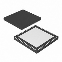
PIC32MX534F064HT-I/MR Microchip Technology, PIC32MX534F064HT-I/MR Datasheet - Page 137

PIC32MX534F064HT-I/MR
Manufacturer Part Number
PIC32MX534F064HT-I/MR
Description
64 PINS, 64KB Flash,16KB RAM, 80 MHz, USB, CAN, 4 DMA 64 QFN 9x9x0.9mm T/R
Manufacturer
Microchip Technology
Series
PIC® 32MXr
Datasheet
1.PIC32MX575F256H-80IMR.pdf
(254 pages)
Specifications of PIC32MX534F064HT-I/MR
Core Processor
MIPS32® M4K™
Core Size
32-Bit
Speed
80MHz
Connectivity
CAN, I²C, SPI, UART/USART, USB OTG
Peripherals
Brown-out Detect/Reset, DMA, POR, PWM, WDT
Number Of I /o
53
Program Memory Size
64KB (64K x 8)
Program Memory Type
FLASH
Ram Size
16K x 8
Voltage - Supply (vcc/vdd)
2.3 V ~ 3.6 V
Data Converters
A/D 16x10b
Oscillator Type
Internal
Operating Temperature
-40°C ~ 85°C
Package / Case
64-VFQFN Exposed Pad
Processor Series
PIC32MX5x
Core
MIPS32
Data Bus Width
32 bit
Data Ram Size
16 KB
Interface Type
I2C, SPI, USART
Maximum Clock Frequency
80 MHz
Number Of Programmable I/os
53
Number Of Timers
5
Operating Supply Voltage
2.3 V to 3.6 V
Maximum Operating Temperature
+ 85 C
Mounting Style
SMD/SMT
Lead Free Status / RoHS Status
Lead free / RoHS Compliant
Eeprom Size
-
Lead Free Status / Rohs Status
Details
- Current page: 137 of 254
- Download datasheet (6Mb)
16.0
FIGURE 16-1:
© 2010 Microchip Technology Inc.
Note 1: This data sheet summarizes the features
Note 1: Where ‘x’ is shown, reference is made to the registers associated with the respective output compare channels,
2: Some registers and associated bits
OUTPUT COMPARE
2: The OCFA pin controls the OC1-OC4 channels. The OCFB pin controls the OC5 channel.
3: Each output compare channel can use one of two selectable 16-bit time bases or a single 32-bit timer base.
of the PIC32MX5XX/6XX/7XX family of
devices. It is not intended to be a
comprehensive reference source. To
complement the information in this data
sheet, refer to Section 16. “Output
Capture”
Family Reference Manual” , which is
available from the Microchip web site
(www.microchip.com/PIC32).
described in this section may not be
available on all devices. Refer to
Section 4.0 “Memory Organization”
this data sheet for device-specific register
and bit information.
1 through 5.
16
TMR Register Inputs
from Time Bases
Comparator
OUTPUT COMPARE MODULE BLOCK DIAGRAM
OCxRS
0
OCxR
(DS61111) in the “PIC32
(1)
(1)
1
16
(3)
OCTSEL
Period Match Signals
from Time Bases
0
in
1
(3)
Mode Select
OCM<2:0>
The Output Compare module (OCMP) is used to gen-
erate a single pulse or a train of pulses in response to
selected time base events. For all modes of operation,
the OCMP module compares the values stored in the
OCxR and/or the OCxRS registers to the value in the
selected timer. When a match occurs, the OCMP
module generates an event based on the selected
mode of operation.
The following are some of the key features:
• Multiple Output Compare Modules in a device
• Programmable interrupt generation on compare
• Single and Dual Compare modes
• Single and continuous output pulse generation
• Pulse-Width Modulation (PWM) mode
• Hardware-based PWM Fault detection and
• Programmable selection of 16-bit or 32-bit time
• Can operate from either of two available 16-bit
PIC32MX5XX/6XX/7XX
event
automatic output disable
bases
time bases or a single 32-bit time base
Output
3
Logic
Set Flag bit
OCxIF
(1)
Output
Enable
R
S
Q
Output Enable
Logic
OCFA or OCFB
OCx
DS61156F-page 137
(1)
(2)
Related parts for PIC32MX534F064HT-I/MR
Image
Part Number
Description
Manufacturer
Datasheet
Request
R

Part Number:
Description:
Manufacturer:
Microchip Technology Inc.
Datasheet:

Part Number:
Description:
Manufacturer:
Microchip Technology Inc.
Datasheet:

Part Number:
Description:
Manufacturer:
Microchip Technology Inc.
Datasheet:

Part Number:
Description:
Manufacturer:
Microchip Technology Inc.
Datasheet:

Part Number:
Description:
Manufacturer:
Microchip Technology Inc.
Datasheet:

Part Number:
Description:
Manufacturer:
Microchip Technology Inc.
Datasheet:

Part Number:
Description:
Manufacturer:
Microchip Technology Inc.
Datasheet:

Part Number:
Description:
Manufacturer:
Microchip Technology Inc.
Datasheet:


