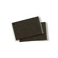
S29JL032H70TFI020 Spansion Inc., S29JL032H70TFI020 Datasheet - Page 27

S29JL032H70TFI020
Manufacturer Part Number
S29JL032H70TFI020
Description
IC,EEPROM,NOR FLASH,2MX16/4MX8,CMOS,TSSOP,48PIN,PLASTIC
Manufacturer
Spansion Inc.
Datasheets
1.S29JL032H70TFI020.pdf
(66 pages)
2.S29JL032H70TFI020.pdf
(66 pages)
3.S29JL032H70TFI020.pdf
(64 pages)
4.S29JL032H70TFI020.pdf
(66 pages)
Specifications of S29JL032H70TFI020
Data Bus Width
8 bit, 16 bit
Architecture
Boot Sector
Interface Type
Conventional
Access Time
70 ns
Supply Voltage (max)
3.6 V
Supply Voltage (min)
2.7 V
Maximum Operating Current
2 mA
Mounting Style
SMD/SMT
Memory Type
Flash
Memory Size
32 Mbit
Operating Temperature
+ 85 C
Package / Case
TSOP-48
Lead Free Status / RoHS Status
Lead free / RoHS Compliant
Lead Free Status / RoHS Status
Lead free / RoHS Compliant
Available stocks
Company
Part Number
Manufacturer
Quantity
Price
Company:
Part Number:
S29JL032H70TFI020H
Manufacturer:
SPANSION
Quantity:
30
Common Flash Memory Interface (CFI)
May 21, 2004 S29JL032HA0
mode. Subsequent writes are ignored until V
must provide the proper signals to the control pins to prevent unintentional writes
when V
Write Pulse “Glitch” Protection
Noise pulses of less than 5 ns (typical) on OE#, CE# or WE# do not initiate a write
cycle.
Logical Inhibit
Write cycles are inhibited by holding any one of OE# = V
V
logical one.
Power-Up Write Inhibit
If WE# = CE# = V
commands on the rising edge of WE#. The internal state machine is automatically
reset to the read mode on power-up.
The Common Flash Interface (CFI) specification outlines device and host system
software interrogation handshake, which allows specific vendor-specified soft-
ware algorithms to be used for entire families of devices. Software support can
then be device-independent, JEDEC ID-independent, and forward- and back-
ward-compatible for the specified flash device families. Flash vendors can
standardize their existing interfaces for long-term compatibility.
This device enters the CFI Query mode when the system writes the CFI Query
command, 98h, to address 55h in word mode (or address AAh in byte mode), any
time the device is ready to read array data. The system can read CFI information
at the addresses given in Tables 9–12. To terminate reading CFI data, the system
must write the reset command.The CFI Query mode is not accessible when the
device is executing an Embedded Program or embedded Erase algorithm.
The system can also write the CFI query command when the device is in the au-
toselect mode. The device enters the CFI query mode, and the system can read
CFI data at the addresses given in Tables 9–12. The system must write the reset
command to reading array data.
For further information, please refer to the CFI Specification and CFI Publication
100. Contact your local sales office for copies of these documents.
IH
. To initiate a write cycle, CE# and WE# must be a logical zero while OE# is a
CC
A D V A N C E
is greater than V
IL
and OE# = V
LKO
I N F O R M A T I O N
.
IH
S29JL032H
during power up, the device does not accept
CC
is greater than V
IL
, CE# = V
LKO
. The system
IH
or WE# =
27


