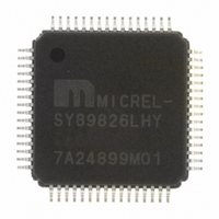
SY89826LHY Micrel Inc, SY89826LHY Datasheet - Page 4

SY89826LHY
Manufacturer Part Number
SY89826LHY
Description
3.3V 1:22 LVDS Fanout/Translator (I Temp, )
Manufacturer
Micrel Inc
Type
Fanout Buffer (Distribution), Multiplexer , Translatorr
Series
Precision Edge®r
Datasheet
1.SY89826LHY.pdf
(10 pages)
Specifications of SY89826LHY
Number Of Circuits
1
Ratio - Input:output
2:22
Differential - Input:output
Yes/Yes
Input
LVDS, LVPECL
Output
LVDS
Frequency - Max
1GHz
Voltage - Supply
3 V ~ 3.6 V
Operating Temperature
-40°C ~ 85°C
Mounting Type
Surface Mount
Package / Case
64-TQFP Exposed Pad, 64-eTQFP, 64-HTQFP, 64-VQFP
Frequency-max
1GHz
Number Of Clock Inputs
2
Mode Of Operation
Differential
Output Frequency
1000MHz
Output Logic Level
LVDS
Operating Supply Voltage (min)
3V
Operating Supply Voltage (typ)
3.3V
Operating Supply Voltage (max)
3.6V
Package Type
TQFP
Operating Temp Range
-40C to 85C
Operating Temperature Classification
Industrial
Signal Type
LVDS/LVPECL
Mounting
Surface Mount
Pin Count
64
Lead Free Status / RoHS Status
Lead free / RoHS Compliant
Other names
576-2567
SY89826LHY
SY89826LHY
Available stocks
Company
Part Number
Manufacturer
Quantity
Price
Company:
Part Number:
SY89826LHY
Manufacturer:
MICREL
Quantity:
1 524
Micrel, Inc.
LVPECL Input:
Symbol
V
V
V
V
I
I
Note 6.
Note 7.
CMOS/LVTTL Inputs:
Symbol
V
V
I
I
LVDS Output
Symbol
V
V
V
V
Note 8.
Note 9.
M9999-011907
hbwhelp@micrel.com or (408) 955-1690
IH
IL
IH
IL
IH
IL
PP
CMR
IH
IL
OD
OH
OL
OCM
V
DC ELECTRICAL CHARACTERISTICS
OCM
The V
V
numbers in the table are referenced to V
equal to V
Measured as per Figure 3, 100 across Q and /Q outputs.
Measured as per Figure 4.
CMR
PP
is defined as the range within which the V
Parameter
Input HIGH Voltage (Single-Ended)
Input LOW Voltage
Minimum Input Swing (LVPECL_CLK)
Common Mode Range (LVPECL_CLK) Note 7
Input HIGH Current
Input LOW Current
Parameter
Input HIGH Voltage
Input LOW Voltage
Input HIGH Current
Input LOW Current
Parameter
Differential Output Voltage
Output HIGH Voltage
Output LOW Voltage
Output Common Mode Voltage
Change in Common Mode Voltage
:
V
(min.) is defined as the minimum input differential voltage which will cause no increase in the propagation delay.
PP
CC
V
(min.). V
CC
= 3.3V 10%, T
= 3.3V 10%, T
V
CC
CMR
= 3.3V 10%, T
range varies 1:1 with V
A
= –40 C to +85 C
A
= –40 C to +85 C
CCI
A
. The V
= –40 C to +85 C
IH
CCI
level may vary, with the device still meeting the propagation delay specification. The
Condition
Note 6
Condition
V
V
Condition
Note 8, 9
Note 8
Note 8
Note 9
IL
IN
IN
. V
level must be such that the peak-to-peak voltage is less than 1.0V and greater than or
= V
= 0.5V
CMR
CC
(min) is fixed at GNDI +1.8V.
4
V
V
GNDI +1.8
CC
CC
0.925
1.125
–600
Min
Min
Min
300
250
–50
0.5
2.0
–1.165
–1.945
Typ
Typ
Typ
350
V
V
V
CC
CC
Precision Edge
CCI
1.474
1.375
Max
Max
Max
150
150
400
0.8
–0.880
–1.625
50
–0.4
SY89826L
Units
Units
Units
mV
mV
mV
V
V
V
V
V
V
V
V
A
A
A
A
®


