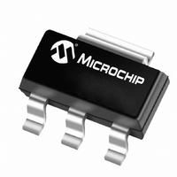
TC1264-3.3VDB Microchip Technology, TC1264-3.3VDB Datasheet - Page 3

TC1264-3.3VDB
Manufacturer Part Number
TC1264-3.3VDB
Description
Analog IC
Manufacturer
Microchip Technology
Specifications of TC1264-3.3VDB
Regulator Topology
Positive Fixed
Voltage - Output
3.3V
Voltage - Input
Up to 6V
Voltage - Dropout (typical)
1.2V @ 800mA
Number Of Regulators
1
Current - Output
800mA (Min)
Operating Temperature
-40°C ~ 125°C
Mounting Type
Surface Mount
Package / Case
SOT-223 (3 leads + Tab), SC-73, TO-261
Number Of Outputs
1
Polarity
Positive
Input Voltage Max
6 V
Output Voltage
3.3 V
Output Type
Fixed
Dropout Voltage (max)
0.03 V at 100 uA
Output Current
800 mA
Line Regulation
0.001 %
Load Regulation
0 % / mA
Voltage Regulation Accuracy
0.5 %
Maximum Operating Temperature
+ 125 C
Mounting Style
SMD/SMT
Minimum Operating Temperature
- 40 C
Lead Free Status / RoHS Status
Lead free / RoHS Compliant
Current - Limit (min)
-
Lead Free Status / Rohs Status
Lead free / RoHS Compliant
Available stocks
Company
Part Number
Manufacturer
Quantity
Price
Company:
Part Number:
TC1264-3.3VDB
Manufacturer:
MICROCHIP
Quantity:
12 000
Company:
Part Number:
TC1264-3.3VDBTR
Manufacturer:
MICROCHIP
Quantity:
15 600
Company:
Part Number:
TC1264-3.3VDBTR
Manufacturer:
SILICON
Quantity:
4 600
Part Number:
TC1264-3.3VDBTR
Manufacturer:
MIC
Quantity:
20 000
DC CHARACTERISTICS (CONTINUED)
TEMPERATURE CHARACTERISTICS
2010 Microchip Technology Inc.
Electrical Specifications: Unless otherwise indicated, V
T
Thermal Regulation
Output Noise
Note 1:
Electrical Specifications: Unless otherwise indicated, V
Temperature Ranges
Specified Temperature Range
Operating Temperature Range
Storage Temperature Range
Thermal Package Resistances
Thermal Resistance, 3L-SOT-223
Thermal Resistance, 3L-DDPAK
Thermal Resistance, 3L-TO-220
Note 1:
A
= +25°C. Boldface type specifications apply for junction temperatures of -40°C to +125°C.
2:
3:
4:
5:
6:
7:
8:
Parameters
V
The minimum V
This accuracy represents the worst-case over the entire output current and temperature range.
Regulation is measured at a constant junction temperature using low duty cycle pulse testing. Load regulation is tested
over a load range from 0.1 mA to the maximum specified output current. Changes in output voltage due to heating
effects are covered by the thermal regulation specification.
Dropout voltage is defined as the input-to-output differential at which the output voltage drops 2% below its nominal
value measured at a 1.5V differential.
Thermal regulation is defined as the change in output voltage at a time T after a change in power dissipation is applied,
excluding load or line regulation effects. Specifications are for a current pulse equal to I
The maximum allowable power dissipation is a function of ambient temperature, the maximum allowable junction
temperature and the thermal resistance from junction-to-air (i.e., T
dissipation causes the device to initiate thermal shutdown. Please see
more details.
Operation in this range must not cause T
TCV
R
is the regulator output voltage setting.
Parameters
OUT
=
------------------------------------------------------------------------ -
V
IN
OUTMAX
has to justify the conditions: V
V
V
OUT
–
OUT
V
Sym
eN
OUTMIN
/P
T
D
10
Sym
–
T
T
T
JA
JA
JA
J
A
A
J
to exceed Maximum Junction Temperature (+125°C).
Min
—
6
—
IN
IN
= V
= V
IN
V
R
R
Min
-40
-40
-65
—
—
—
+ 1.5V,
+ 1.5V, I
R
+ V
0.04
Typ
260
DROPOUT
(Note
L
Typ
59
71
71
—
—
—
= 100 µA, C
A
, T
1), I
Max
and V
J
—
—
,
L
Section 5.0 “Thermal Considerations”
+125
+125
+150
Max
= 100 µA, C
JA
—
—
—
). Exceeding the maximum allowable power
L
IN
= 3.3 µF, SHDN > V
2.7V for I
nV/Hz
Units
V/W
Units
°C/W
°C/W
°C/W
°C
°C
°C
L
= 3.3 µF, SHDN > V
LMAX
Note 7
I
L
L
= 0.1 mA to I
= I
(Note
at V
OUTMAX
IH
IN
TC1264
Conditions
, T
1)
= 6V for T = 10 ms.
Conditions
A
DS21375D-page 3
, F = 10 kH
= +25°C.
OUTMAX
IH
,
.
for
Z


