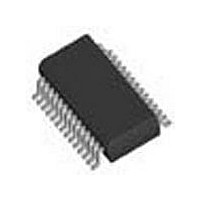
PI6C182HEX Pericom Semiconductor, PI6C182HEX Datasheet - Page 3

PI6C182HEX
Manufacturer Part Number
PI6C182HEX
Description
Clock Buffer Precision 1 12 Clock Buffer
Manufacturer
Pericom Semiconductor
Datasheet
1.PI6C182HE.pdf
(7 pages)
Specifications of PI6C182HEX
Number Of Outputs
10
Max Input Freq
110 MHz
Propagation Delay (max)
5.5 ns
Supply Voltage (max)
3.465 V
Supply Voltage (min)
3.135 V
Maximum Operating Temperature
+ 70 C
Minimum Operating Temperature
0 C
Mounting Style
SMD/SMT
Package / Case
SSOP-28
Operating Supply Voltage (max)
3.465V
Operating Temp Range
0C to 70C
Propagation Delay Time
8ns
Operating Supply Voltage (min)
3.135V
Mounting
Surface Mount
Pin Count
28
Operating Supply Voltage (typ)
3.3V
Package Type
SSOP
Input Frequency
110MHz
Duty Cycle
55%
Operating Temperature Classification
Commercial
Lead Free Status / RoHS Status
Compliant
Lead Free Status / RoHS Status
Lead free / RoHS Compliant, Compliant
2-Wire I
The I
output and test mode enable.
The PI6C182 is a slave receiver device. It can not be read back.
Sub-addressing is not supported. All preceding bytes must be sent
in order to change one of the control bytes.
Each byte on the SDATA line must be 8-bits long (MSB fi rst), fol-
lowed by an acknowledge bit generated by the re ceiver.
During normal data transfers SDATA changes only when SCLOCK
is LOW. Exceptions: A HIGH to LOW transition on SDATA while
SCLOCK is HIGH indicates a “start” condition. A LOW to HIGH
transition on SDATA while SCLOCK is HIGH indicates a “stop”
condition and in di cates the end of a data transfer cycle.
Each data transfer is initiated with a start condition and ends with
a stop condition. The fi rst byte after a start condition is always a
Byte1: SDRAM Active/Inactive Reg is ter
(1 = enable, 0 = disable)
Maximum Ratings
Supply Current
Storage Temperature ............................................................–65°C to +150°C
Ambient Temperature with Power Applied .............................–0°C to +70°C
3.3V Supply Voltage to Ground Potential ..............................–0.5V to +4.6V
DC Input Voltage ....................................................................–0.5V to +4.6V
Bit
7
6
5
4
3
2
1
0
2
Symbol
C interface permits individual enable/disable of each clock
I
I
I
I
08-0298
DD
DD
DD
DD
2
Pin
C Control
27
26
23
22
Description
SDRAM7 (Active/Inactive)
SDRAM6 (Active/Inactive)
SDRAM5 (Active/Inactive)
SDRAM4 (Active/Inactive)
NC (Initialize to 0)
NC (Initialize to 0)
NC (Initialize to 0)
NC (Initialize to 0)
(V
DD
= +3.465V, C
Supply Current
Parameter
LOAD
= Max.)
Test Condidtion
BUF_IN = 0 MHz
BUF_IN = 66.66 MHz
BUF_IN = 100.00 MHz
BUF_IN = 133.00 MHz
3
7-bit address byte followed by a read/write bit. (HIGH = read from
addressed device, LOW = write to ad dressed device). If the de vice’s
own address is detected, PI6C182 gen er ates an ac knowl edge by
pulling SDATA line LOW during ninth clock pulse, then accepts
the fol low ing data bytes until another start or stop con di tion is
detected.
Following acknowledgement of the address byte (D2), two more
bytes must be sent:
1. “Command Code” byte
2. “Byte Count” byte.
Although the data bits on these two bytes are “don’t care,” they
must be sent and acknowledged.
Byte2: Optional Register for Possible Future
Requirements (1 = enable, 0 = disable)
Bit
7
6
5
4
3
2
1
0
Pin
18
11
Note:
Stresses greater than those listed under MAX I MUM RAT-
INGS may cause permanent damage to the de vice. This is
a stress rating only and functional operation of the device
at these or any other con di tions above those indicated in
the operational sec tions of this spec i fi ca tion is not implied.
Ex po sure to absolute maximum rating conditions for ex-
tend ed periods may affect re li abil i ty.
Description
SDRAM9 (Active/Inactive)
SDRAM8 (Active/Inactive)
(Reserved)
(Reserved)
(Reserved)
(Reserved)
(Reserved)
(Reserved)
Min.
Precision 1-to-10 Clock Buffer
Typ.
PI6C182, PI6C182A
Max.
180
240
360
2
PS8165G
Units
mA
11/13/08


