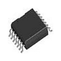
MF6CWM-100 National Semiconductor, MF6CWM-100 Datasheet - Page 18

MF6CWM-100
Manufacturer Part Number
MF6CWM-100
Description
Manufacturer
National Semiconductor
Datasheet
1.MF6CWM-100.pdf
(20 pages)
Specifications of MF6CWM-100
Architecture
Switched Capacitor
Dual Supply Voltage (typ)
±3/±5V
Power Supply Requirement
Single/Dual
Single Supply Voltage (min)
5V
Dual Supply Voltage (min)
±2.5V
Operating Temperature (min)
0C
Operating Temperature (max)
70C
Operating Temperature Classification
Commercial
Package Type
SOIC W
Filter Type
Low Pass Filter
Lead Free Status / RoHS Status
Not Compliant
Available stocks
Company
Part Number
Manufacturer
Quantity
Price
Company:
Part Number:
MF6CWM-100
Manufacturer:
NS
Quantity:
5 510
Company:
Part Number:
MF6CWM-100
Manufacturer:
QTC
Quantity:
5 510
Part Number:
MF6CWM-100
Manufacturer:
NS/国半
Quantity:
20 000
www.national.com
2.0 Designing with the MF6
f
2.5 ALIASING CONSIDERATIONS
Aliasing effects have to be taken into consideration when in-
put signal frequencies exceed half the sampling rate. For the
MF6 this equals half the clock frequency (f
put signal contains a component at a frequency higher than
half the clock frequency, as in Figure 19a , that component
will be “reflected” about f
low f
IN
FIGURE 17. MF6-50 Abrupt Clock Frequency Change
FIGURE 19. The phenomenon of aliasing in sampled-data systems. An input signal whose frequecy is greater than
= 1.5 kHz (scope time base = 2 ms/div)
one-half the sampling frequency will cause an output to appear at a frequency lower than one-half the sampling
CLK
/2 as in Figure 19b . If this component is within the
(a) Input Signal Spectrum
CLK
/2 into the frequency range be-
CLK
). When the in-
DS005065-37
(Continued)
frequency. In the MF6, f
DS005065-30
18
at f
(b) Output Signal Spectrum. Note that the input signal
s
/2 + f causes an output signal to appear at f
passband of the filter and of large enough amplitude it can
cause problems. Therefore if frequency components in the
input signal exceed f
being applied to the MF6 input. The necessary amount of at-
tenuation will vary depending on system requirements. In
critical applications the signal components above f
have to be attenuated at least to the filter’s residual noise
level. An example circuit is shown in Figure 20 using one of
the uncommitted Op-Amps available in the MF6.
FIGURE 18. MF6-50 Step Input Response, Vertical =
2V/div., Horizontal = 1 ms/div., f
s
f
CLK
.
CLK
/2 they must be attenuated before
CLK
DS005065-38
= 100 kHz
s
/2 − f.
CLK
DS005065-31
/2 will


