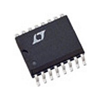
LTC1264-7CSW#TRMPBF Linear Technology, LTC1264-7CSW#TRMPBF Datasheet - Page 10

LTC1264-7CSW#TRMPBF
Manufacturer Part Number
LTC1264-7CSW#TRMPBF
Description
Manufacturer
Linear Technology
Datasheet
1.LTC1264-7CSWTRMPBF.pdf
(16 pages)
Specifications of LTC1264-7CSW#TRMPBF
Order Filter (max)
8th
Single Supply Voltage (typ)
5/9/12/15V
Dual Supply Voltage (typ)
±3/±5V
Power Supply Requirement
Single/Dual
Single Supply Voltage (min)
4.75V
Single Supply Voltage (max)
16V
Dual Supply Voltage (min)
±2.375V
Dual Supply Voltage (max)
±8V
Operating Temperature (min)
-40C
Operating Temperature (max)
85C
Package Type
SOIC W
Filter Type
Low Pass Filter
Lead Free Status / RoHS Status
Compliant
PI FU CTIO S
LTC1264-7
NC Pin (1, 5, 8, 13)
Pins 1, 5, 8 and 13 are not connected to any internal circuit
point on the device and should be preferably tied to analog
ground.
Filter Input Pin (2)
The input pin is connected internally through a 50k resis-
tor tied to the inverting input of an op amp.
Analog Ground Pins (3, 5)
The filter performance depends on the quality of the
analog signal ground. For either dual or single supply
operation, an analog ground plane surrounding the pack-
age is recommended. The analog ground plane should be
connected to any digital ground at a single point. For dual
supply operation, pin 3 should be connected to the analog
ground plane. For single supply operation pin 3 should be
biased at 1/2 supply and should be bypassed to the analog
ground plane with at least a 1µF capacitor (Figure 3). For
single 5V operation at the highest f
should be biased at 2V. This minimizes passband gain and
phase variations.
Power Supply Pins (4, 12)
The V
bypassed with a 0.1µF capacitor to an adequate analog
ground. The filter’s power supplies should be isolated
from other digital or high voltage analog supplies. A low
noise linear supply is recommended. Using a switching
power supply will lower the signal-to-noise ratio of the
filter. The supply during power-up should have a slew rate
less than 1V/µs. When V
allowed to go above ground, a signal diode should clamp
V
connections for dual and single supply operation.
10
–
U
to prevent latch-up. Figures 2 and 3 show typical
+
(pin 4) and the V
U
U
+
is applied before V
–
(pin 12) should each be
CLK
of 2MHz, pin 3
–
and V
–
is
Filter Output Pins (6, 9)
Pin 9 is the specified output of the filter; it can typically
source 3mA and sink 1mA. Driving coaxial cables or
resistive loads less than 20k will degrade the total har-
monic distortion of the filter. When evaluating the device’s
distortion an output buffer is required. A noninverting
buffer, Figure 4, can be used provided that its input
common-mode range is well within the filter’s output
swing. Pin 6 is an intermediate filter output providing an
unspecified 6th order lowpass filter. Pin 6 should not be
loaded.
V
V
V
V
Figure 3. Single Supply Operation for an f
IN
10k
10k
IN
+
Figure 2. Dual Supply Operation for an f
+
0.1µF
0.1µF
Figure 4. Buffer for Filter Output
1
2
3
4
5
6
7
+
LTC1264-7
1
2
3
4
5
6
7
1k
1µF
LTC1264-7
–
+
LT1220
14
13
12
11
10
9
8
V
+
14
13
12
11
10
9
8
0.1µF
1264-7 F04
200Ω
V
200Ω
CLK
+
CLK
/f
V
V
/f
CUTOFF
OUT
–
CUTOFF
DIGITAL SUPPLY
CLOCK SOURCE
GND
DIGITAL SUPPLY
V
CLOCK SOURCE
GND
OUT
= 25:1
= 25:1
1264-7 F02
1264-7 F03
+
12647fa
+


