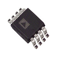
AD5220BRM10-REEL7 Analog Devices Inc, AD5220BRM10-REEL7 Datasheet - Page 3

AD5220BRM10-REEL7
Manufacturer Part Number
AD5220BRM10-REEL7
Description
Manufacturer
Analog Devices Inc
Datasheet
1.AD5220BRM10-REEL7.pdf
(11 pages)
Specifications of AD5220BRM10-REEL7
Number Of Elements
1
# Of Taps
128
Resistance (max)
10KOhm
Power Supply Requirement
Single
Interface Type
Serial (3-Wire)
Single Supply Voltage (typ)
3/5V
Dual Supply Voltage (typ)
Not RequiredV
Single Supply Voltage (min)
2.7V
Single Supply Voltage (max)
5.5V
Dual Supply Voltage (min)
Not RequiredV
Dual Supply Voltage (max)
Not RequiredV
Operating Temp Range
-40C to 85C
Operating Temperature Classification
Industrial
Mounting
Surface Mount
Pin Count
8
Package Type
MSOP
Lead Free Status / RoHS Status
Not Compliant
Available stocks
Company
Part Number
Manufacturer
Quantity
Price
Part Number:
AD5220BRM10-REEL7
Manufacturer:
ADI/亚德诺
Quantity:
20 000
ABSOLUTE MAXIMUM RATINGS*
(T
V
V
A
Digital Input Voltage to GND . . . . . . . . . . . 0 V, V
Operating Temperature Range . . . . . . . . . . . –40 C to +85 C
Maximum Junction Temperature (T
Storage Temperature . . . . . . . . . . . . . . . . . . –65 C to +150 C
Lead Temperature (Soldering, 10 sec) . . . . . . . . . . . . +300 C
Package Power Dissipation . . . . . . . . . . . . . . (T
Thermal Resistance
*Stresses above those listed under Absolute Maximum Ratings
CAUTION
ESD (electrostatic discharge) sensitive device. Electrostatic charges as high as 4000 V readily
accumulate on the human body and test equipment and can discharge without detection.
Although the AD5220 features proprietary ESD protection circuitry, permanent damage may
occur on devices subjected to high energy electrostatic discharges. Therefore, proper ESD
precautions are recommended to avoid performance degradation or loss of functionality.
REV.
CS
L
L
H
permanent damage to the device. This is a stress rating only; functional operation
of the device at these or any other conditions above those indicated in the
operational sections of this specification is not implied. Exposure to absolute
maximum rating conditions for extended periods may affect device reliability.
DD
A
X
A
P-DIP (N-8) . . . . . . . . . . . . . . . . . . . . . . . . . . . . 103 C/W
SOIC (SO-8) . . . . . . . . . . . . . . . . . . . . . . . . . . . . 158 C/W
, V
–B
SOIC (RM-8) . . . . . . . . . . . . . . . . . . . . . . . . . . . 206 C/W
= +25 C, unless otherwise noted)
to GND . . . . . . . . . . . . . . . . . . . . . . . . . . . . –0.3 V, +7 V
B
X
A
, V
, A
CLK U/D
t
t
X
CLK
U/D
CS
W
X
–W
1
0
1
0
1
0
to GND . . . . . . . . . . . . . . . . . . . . . . . . . . 0 V, V
X
Figure 3. Detail Timing Diagram
, B
H
L
X
X
–W
t
t
t
Table I. Truth Table
JA
CL
CSS
UDS
X
Operation
Wiper Increment Toward Terminal A
Wiper Decrement Toward Terminal B
Wiper Position Fixed
. . . . . . . . . . . . . . . . . . . . . .
t
CH
J
MAX) . . . . . . . . +150 C
J
t
max–T
CSH
DD
may cause
+ 0.3 V
20 mA
A
)/
DD
JA
–3–
Pin
No.
1
2
3
4
5
6
7
8
Name
CLK
U/D
A1
GND
W1
B1
CS
V
DD
PIN FUNCTION DESCRIPTIONS
Description
Serial Clock Input, Negative Edge Triggered
UP/DOWN Direction Increment Control
Terminal A1
Ground
Wiper Terminal
Terminal B1
Chip Select Input, Active Low
Positive Power Supply
PIN CONFIGURATION
GND
CLK
U/D
A1
1
2
3
4
(Not to Scale)
TOP VIEW
AD5220
WARNING!
8
7
6
5
V
CS
B1
W1
DD
ESD SENSITIVE DEVICE
AD5220


