DS90LV031BTM National Semiconductor, DS90LV031BTM Datasheet - Page 5
DS90LV031BTM
Manufacturer Part Number
DS90LV031BTM
Description
01C8071
Manufacturer
National Semiconductor
Datasheet
1.DS90LV031BTM.pdf
(10 pages)
Specifications of DS90LV031BTM
Number Of Elements
4
Input Type
CMOS/TTL
Operating Supply Voltage (typ)
3.3V
Differential Output Voltage
450mV
Propagation Delay Time
2ns
Power Dissipation
1.088W
Operating Temp Range
-40C to 85C
Operating Temperature Classification
Industrial
Mounting
Surface Mount
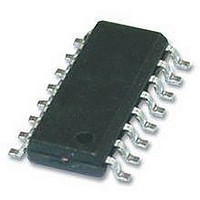
Pin Count
16
Package Type
SOIC N
Number Of Receivers
4
Number Of Drivers
4
Supply Current
23mA
Supply Voltage Range
3V To 3.6V
Driver Case Style
SOIC
No. Of Pins
16
Operating Temperature Range
-40°C To +85°C
Device Type
Differential Line Driver
Rohs Compliant
No
Data Rate Max
400Mbps
Lead Free Status / RoHS Status
Not Compliant
Available stocks
Company
Part Number
Manufacturer
Quantity
Price
Company:

Part Number:
DS90LV031BTM
Manufacturer:
NS
Quantity:
2
Company:
Part Number:
DS90LV031BTMX
Manufacturer:
NSC
Quantity:
6 613


Typical Application
Applications Information
General application guidelines and hints for LVDS drivers and
receivers may be found in the following application notes:
LVDS Owner's Manual (lit #550062-001), AN808, AN977,
AN971, AN916, AN805, AN903.
LVDS drivers and receivers are intended to be primarily used
in an uncomplicated point-to-point configuration as is shown
in Figure 6. This configuration provides a clean signaling en-
vironment for the quick edge rates of the drivers. The receiver
is connected to the driver through a balanced media which
may be a standard twisted pair cable, a parallel pair cable, or
simply PCB traces. Typically, the characteristic differential
impedance of the media is in the range of 100Ω. A termination
resistor of 100Ω should be selected to match the media, and
is located as close to the receiver input pins as possible. The
termination resistor converts the current sourced by the driver
into a voltage that is detected by the receiver. Other configu-
rations are possible such as a multi-receiver configuration,
but the effects of a mid-stream connector(s), cable stub(s),
and other impedance discontinuities as well as ground shift-
ing, noise margin limits, and total termination loading must be
taken into account.
The DS90LV031B differential line driver is a balanced current
source design. A current mode driver, generally speaking has
a high output impedance and supplies a constant current for
a range of loads (a voltage mode driver on the other hand
FIGURE 5. Driver TRI-STATE Delay Waveform
FIGURE 6. Point-to-Point Application
5
supplies a constant voltage for a range of loads). Current is
switched through the load in one direction to produce a logic
state and in the other direction to produce the other logic state.
The output current is typically 3.5 mA, a minimum of 2.5 mA,
and a maximum of 4.5 mA. The current mode requires (as
discussed above) that a resistive termination be employed to
terminate the signal and to complete the loop as shown in
Figure 6. AC or unterminated configurations are not allowed.
The 3.5 mA loop current will develop a differential voltage of
350 mV across the 100Ω termination resistor which the re-
ceiver detects with a 250 mV minimum differential noise
margin neglecting resistive line losses (driven signal minus
receiver threshold (350 mV – 100 mV = 250 mV)). The signal
is centered around +1.2V (Driver Offset, V
ground as shown in Figure 7. Note that the steady-state volt-
age (V
(V
The current mode driver provides substantial benefits over
voltage mode drivers, such as an RS-422 driver. Its quiescent
current remains relatively flat versus switching frequency.
Whereas the RS-422 voltage mode driver increases expo-
nentially in most case between 20 MHz–50 MHz. This is due
to the overlap current that flows between the rails of the device
when the internal gates switch. Whereas the current mode
driver switches a fixed current between its output without any
substantial overlap current. This is similar to some ECL and
PECL devices, but without the heavy static I
OD
) and is typically 700 mV.
SS
) peak-to-peak swing is twice the differential voltage
10131108
10131107
OS
CC
) with respect to
requirements
www.national.com
Related parts for DS90LV031BTM
Image
Part Number
Description
Manufacturer
Datasheet
Request
R

Part Number:
Description:
National Semiconductor [8-Bit D/A Converter]
Manufacturer:
National Semiconductor
Datasheet:
Part Number:
Description:
National Semiconductor [Media Coprocessor]
Manufacturer:
National Semiconductor
Datasheet:
Part Number:
Description:
Digitally Controlled Tone and Volume Circuit with Stereo Audio Power Amplifier, Microphone Preamp Stage and National 3D Sound
Manufacturer:
National Semiconductor
Datasheet:
Part Number:
Description:
Digitally Controlled Tone and Volume Circuit with Stereo Audio Power Amplifier, Microphone Preamp Stage and National 3D Sound
Manufacturer:
National Semiconductor
Datasheet:
Part Number:
Description:
AC97 Rev 2 Codec with Sample Rate Conversion and National 3D Sound
Manufacturer:
National Semiconductor
Part Number:
Description:
Manufacturer:
National Semiconductor
Datasheet:
Part Number:
Description:
Manufacturer:
National Semiconductor
Datasheet:
Part Number:
Description:
General Purpose, Low Voltage, Low Power, Rail-to-Rail Output Operational Amplifiers
Manufacturer:
National Semiconductor
Datasheet:
Part Number:
Description:
8-bit 20 MSPS flash A/D converter.
Manufacturer:
National Semiconductor
Datasheet:
Part Number:
Description:
Low Noise Quad Operational Amplifier
Manufacturer:
National Semiconductor
Datasheet:
Part Number:
Description:
Quad Differential Line Receivers
Manufacturer:
National Semiconductor
Datasheet:
Part Number:
Description:
Quad High Speed Trapezoidal? Bus Transceiver
Manufacturer:
National Semiconductor
Datasheet:
Part Number:
Description:
Dual Line Receiver
Manufacturer:
National Semiconductor
Datasheet:
Part Number:
Description:
TTL to 10k ECL Level Translator with Latch
Manufacturer:
National Semiconductor
Datasheet: