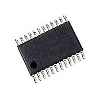
LX5255CPW Semicoa Semiconductors, LX5255CPW Datasheet - Page 2

LX5255CPW
Manufacturer Part Number
LX5255CPW
Description
Manufacturer
Semicoa Semiconductors
Type
SCSI Terminationr
Datasheet
1.LX5255CPW.pdf
(7 pages)
Specifications of LX5255CPW
Number Of Bits
9
Operating Supply Voltage (typ)
3.3/5V
Operating Supply Voltage (max)
5.25V
Package Type
TSSOP
Mounting
Surface Mount
Pin Count
24
Operating Temperature Classification
Commercial
Lead Free Status / RoHS Status
Compliant
Available stocks
Company
Part Number
Manufacturer
Quantity
Price
Company:
Part Number:
LX5255CPW
Manufacturer:
SANYO
Quantity:
5
Part Number:
LX5255CPW
Manufacturer:
MSC
Quantity:
20 000
Copyright © 2000
Rev. 1.1, 2006-02-27
Term Power (V
Signal Line Voltage .............................................................................................-0.3V to 7V
Differential Voltage .............................................................................................-0.3V to 7V
Operating Junction Temperature.................................................................................. 150°C
Storage Temperature Range........................................................................... -65°C to 150°C
Peak Package Solder Reflow Temperature (40 second maximum exposure) . 260°C (+0, -5)
Note:
Signal Line Voltage
VTerm
Disconnect Input Voltage
Operating Junction Temperature
Junction Temperature Calculation: T
The θ
system. All of the above assume no ambient airflow. θ
depending on mounting technique. (See Application Notes Section: Thermal
considerations)
T
H or Open
PW
HERMAL
DISC
L
L
L
JA
Exceeding these ratings could cause damage to the device. All voltages are with respect to
Ground. Currents are positive into, negative out of specified terminal.
TM
numbers are guidelines for the thermal performance of the device/pc-board
DIFFB/POWER UP/POWER DOWN FUNCTION TABLE
24L TSSOP
R
ESISTANCE
TERM
A B S O L U T E M A X I M U M R A T I N G S
0.7V to 1.9V
)............................................................................................-0.3V to 7V
DIFFB
H > 2.4V
L < 0.5V
11861 Western Avenue, Garden Grove, CA. 92841, 714-898-8121, Fax: 714-893-2570
X
-J
T H E R M A L D A T A
Parameter
R E C O M M E N D E D M A X O P E R A T I N G C O N D I T I O N S
UNCTION TO
Status
J
Disable
Disable
Disable
Enable
= T
A
+ (P
A
Outputs
MBIENT
D
x θ
Integrated Products Division
JA
, θ
).
JA
Type
®
Microsemi
JA
HI-Z
LVD
HI-Z
HI-Z
can vary significantly
Quiescent
Symbol
Current
V
30mA
TERM
10µA
T
8mA
8mA
100°C/W
9-Line LVD SCSI Terminator
J
P
RODUCTION DATA SHEET
Min
2.7
0
0
0
RoHS / Pb-free 100% Matte Tin Lead Finish
DIFSENS
LX5255
DIFFB
GND
NC
1+
2+
2-
3+
3-
4+
4-
1-
Typ
P A C K A G E P I N O U T
NC – No Internal Connection
10
11
12
1
2
3
4
5
6
7
8
9
PW P
(Top View)
Max
V
ACKAGE
5.25
5.0
70
TERM
24
23
22
21
20
19
18
17
16
15
14
13
LX5255
Units
VTERM
9-
9+
8-
8+
7-
7+
6-
6+
5-
5+
DISC
°C
V
V
V
Page 2


