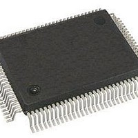
HV257FG Supertex, HV257FG Datasheet - Page 6

HV257FG
Manufacturer Part Number
HV257FG
Description
Sample & Hold Amplifiers 32-CH MEMS Drvr IC
Manufacturer
Supertex
Datasheet
1.HV257FG.pdf
(15 pages)
Specifications of HV257FG
Operating Temperature (max)
85C
Operating Temperature Classification
Commercial
Mounting
Surface Mount
Maximum Operating Temperature
+ 85 C
Minimum Operating Temperature
- 10 C
Mounting Style
SMD/SMT
Package / Case
MQFP-100
Lead Free Status / RoHS Status
Not Compliant
Available stocks
Company
Part Number
Manufacturer
Quantity
Price
Company:
Part Number:
HV257FG-G
Manufacturer:
Supertex
Quantity:
135
Power Up/Down Issues
External Diode Protection
The device can be damaged due to improper power up / down
sequence. To prevent damage, please follow the acceptable
power up / down sequences, and add two external diodes as
shown in the diagram on the right. The first diode is a high
voltage diode across VPP and VDD, where the anode of the
diode is connected to VDD and the cathode of the diode
is connected to VPP. Any low current, high voltage diode,
such as a 1N4004, will be adequate. The second diode is a
Schottky diode across VNN and DGND, where the anode of
the Schottky diode is connected to VNN, and the cathode is
connected to DGND. Any low current Schottky diode such
as a 1N5817 will be adequate.
Acceptable Power Up Sequences
The HV257 can be powered up with any of the following
sequences listed below.
Acceptable Power Down Sequences
The HV257 can be powered down with any of the following
sequences listed below.
Recommended Power Up/Down Timing
HV
OUT
1) VPP 2) VNN 3) VDD 4) Inputs and Anode
1) VNN 2) VDD 3) VPP 4) Inputs and Anode
1) VDD & VNN 2) Inputs 3) VPP 4) Anode
1) Inputs and Anode 2) VDD 3) VNN 4) VPP
1) Inputs and Anode 2) VPP 3) VDD 4) VNN
1) Anode 2) VPP 3) Inputs 4) VNN & VDD
Level at Power Up
HVOUT
VSIG
VDD
VNN
VPP
A
0
HVOUT
- A
EN
VNN
VDD
VPP
4
●
1235 Bordeaux Drive, Sunnyvale, CA 94089
0
VNN Before VDD
1
2 31
Power Up Sequence
0
6.5V
-5.5V
0V
0V
0V
-5.5V
0V
0
6
1
External Diode Protection Connection
Suggested Power Up/Down Sequence
The HV257 needs all power supplies to be fully up and all
channels refreshed with V
outputs to 0V. Before that time, the high voltage outputs
may have temporary voltage excursions above or below
GND level depending on selected power up sequence. To
minimize the excursions:
1. The VDD and VNN power supplies should be applied at
the same time (or within a few nanoseconds).
V
Suggested VPP ramp up speed should be 10msec or longer
and
2. All channels should be continuously refreshed with
HVOUT
SIG
VPP
VDD
VNN
2
= 0V, just before, and while the VPP is ramping up.
ramp down to be 1msec or longer.
VDD Before VNN
●
VDD
VNN
Tel: 408-222-8888
Gnd +/- V offset X 72
Gnd +/- V offset X 72
1N5817 or similar
1N4004 or similar
6.5V
-5.5V
SIG
0V
0V
0V
6.5V
0V
●
= 0V to force all high voltage
www.supertex.com
300V
300V
6.5V
6.5V
-5.5V
-5.5V
0V
0V
0V
0V
0V
0V
0V
0V
0V
0V
DGND
VPP


