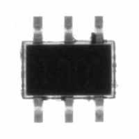
USBUF01W6 STMicroelectronics, USBUF01W6 Datasheet - Page 5

USBUF01W6
Manufacturer Part Number
USBUF01W6
Description
IC EMI FLTR/LINE TERM SOT323-6
Manufacturer
STMicroelectronics
Series
ASDr
Datasheet
1.USBUF02W6.pdf
(11 pages)
Specifications of USBUF01W6
Filter Type
Signal Line
Mounting Type
Surface Mount
Termination Style
Surface Mount (SMD,SMT)
Lead Free Status / RoHS Status
Lead free / RoHS Compliant
Inductance
-
Lead Free Status / Rohs Status
Lead free / RoHS Compliant
Other names
497-3087-2
Available stocks
Company
Part Number
Manufacturer
Quantity
Price
Part Number:
USBUF01W6
Manufacturer:
ST
Quantity:
20 000
USBUFxxW6
Figure 6.
Figure 7.
To have a good approximation of the remaining voltages at both Vin and Vout stages, we
give the typical dynamical resistance value Rd. By taking into account these following
hypothesis: R
The results of the calculation done for V
V
This confirms the very low remaining voltage across the device to be protected. It is also
important to note that in this approximation the parasitic inductance effect was not taken into
account. This could be few tenths of volts during few ns at the V
effect is not present at the V
The measurements done hereafter show very clearly (figure 8) the high efficiency of the
ESD protection:
●
●
BR
Discharge
= 7 V (typ.) and R
Vinput = 31.2 V
Voutput = 7.95 V
no influence of the parasitic inductances on Voutput stage
Voutput clamping voltage very close to V
and - V
SURGE
16kV
ESD
Air
ESD Surge
F
USBUFxxW6 ESD clamping behavior
Measurement board
t
(forward voltage) in the negative way
V
> R
PP
d
, R
Vin
TEST BOARD
g
d
> R
= 1
Rg
d
output
and R
V
(typ.) give:
ouput
Vout
V
Vinput
side due the low current involved after the resistance R
Rd
BR
S1
load
=
> R
g
R
------------------------------------------------------ -
=
Vinput
= 8 kV, R
USBUF01W6
t
d
R
---------------------------------------------- -
, it gives these formulas:
V
g
BR
BR
Rt
Voutput
V
+
BR
(breakdown voltage) in the positive way
R
R
R
t
g
d
+
g
= 330
R
Vinput
d
V
S2
Rd
V
g
BR
(IEC 61000-4-2 standard),
input
Technical information
side. This parasitic
protected
Device
to be
Rload
5/11
t
.


