IPD2132 OSRAM Opto Semiconductors Inc, IPD2132 Datasheet - Page 11
IPD2132
Manufacturer Part Number
IPD2132
Description
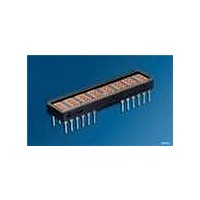
LED Displays 5x7 Super Red 0.2 , 8-CHARACTER
Manufacturer
OSRAM Opto Semiconductors Inc
Series
Alphanumeric Programmable Display™r
Datasheet
1.IPD2131.pdf
(16 pages)
Specifications of IPD2132
Display Type
Dot Matrix
Emitting Color
Hi-Eff. Red
Number Of Digits
8
Digit Size (in)
.2in
Viewing Area Height (mm)
4.8mm
Viewing Area Length (mm)
2.8mm
Package Type
Panel
Operating Supply Voltage (min)
4.5V
Operating Supply Voltage (typ)
5V
Operating Supply Voltage (max)
5.5V
Operating Temperature Classification
Industrial
Operating Temp Range
-55C to 100C
Mounting
Through Hole
Pin Count
24
Total Thickness (mm)
4.6mm
Opto Display Type
Panel
Pattern Type
Dot Matrix
Millicandela Rating
350µcd
Size / Dimension
1.68" L x 0.39" W x 0.21" H (42.7mm x 4.8mm x 5.3mm)
Color
Red
Configuration
5 x 7
Character Size
0.2 in
Illumination Color
High Efficiency Red
Wavelength
635 nm
Maximum Operating Temperature
+ 100 C
Minimum Operating Temperature
- 55 C
Luminous Intensity
350 ucd
Viewing Area (w X H)
2.8 mm x 4.8 mm
Lead Free Status / RoHS Status
Compliant
Voltage - Forward (vf) Typ
-
Internal Connection
-
Lead Free Status / Rohs Status
Details
Other names
Q68000A8836


Character RAM
The Character RAM is selected when FL , A4 and A3 are set to
1,1,1 during a read or write cycle. The Character RAM is a 8 by 8
bit RAM with each of the eight locations corresponding to a digit on
the display. Digit 0 is on the left side of the display and digit 7 is on
the right side of the display. Address lines, A2–A0 select the digit
address with A2 being the most significant bit and A0 being the
least significant bit. The two types of data stored in the Character
RAM are the ASCII coded data and the UDC Address Data. The
type of data stored in the Character RAM is determined by data bit,
D7. If D7 is low, then ASCII coded data is stored in data bits D6–
D0. If D7 is high, then UDC Address Data is stored in data bit D3–
D0.
The ASCII coded data is a 7 bit code used to select one of 128
ASCII characters permanently stored in the ASCII ROM.
The UDC Address data is a 4 bit code used to select one of the
UDC characters in the UDC RAM. There are up to 16 characters
available. See Table „Character RAM Access Logic“ (page 11).
UDC Address Register and UDC RAM
The UDC Address Register and UDC RAM allows the user to gen-
erate and store up to 16 custom characters. Each custom charac-
ter is defined in 5 x 7 dot matrix pattern. It takes 8 write cycles to
define a custom character, one cycle to load the UDC Address
Register and 7 cycles to define the character. The contents of the
UDC Address Register will store the 4 bit address for one of the 16
UDC RAM locations. The UDC RAM is used to store the custom
character.
UDC Address Register
Character RAM Access Logic
RST
1
1
1
1
UDC Address Register and UDC Character RAM
RST
1
1
1
1
2006-04-04
CE
0
0
0
0
CE
0
0
0
0
WR
0
1
0
1
WR
0
1
0
1
RD
1
0
1
0
RD
1
0
1
0
FL
1
1
1
1
FL
1
1
1
1
A4
1
1
0
0
A4
0
0
0
0
A3
1
1
0
0
A3
0
0
1
1
A2
Character Address for
Digits 0–7
Character Address for
Digits 0–7
Character Address for
Digits 0–7
Character Address for
Digits 0–7
A2
Not used for UDC
Address Register
Not used for UDC
Address Register
A2–A0=Character
Row Address
A2–A0=Character
Row Address
11
The UDC Address Register is selected by setting FL=1, A4=0,
A3=0. It is a 4 bit register and uses data bits, D3–D0 to store the
4 bit address code (D7–D4 are ignored). The address code
selects one of 16 UDC RAM locations for custom character gen-
eration.
UDC RAM
The UDC RAM is selected by setting FL=1, A4=0, A3=1. The RAM
is comprised of a 7 x 5 bit RAM. As shown in Table „UDC Charac-
ter Map“ (page 12), address lines, A2-A0 select one of the 7 rows
of the custom character. Data bits, D4-D0 determine the 5 bits of
column data in each row. Each data bit corresponds to a LED. If
the data bit is high, then the LED is on. If the data bit is low, the
LED is off. To create a character, each of the 7 rows of column
data need to be defined. See Tables „UDC Address Register and
UDC RAM“ (page 11) and „UDC Character Map“ (page 12) for
logic.
Flash RAM
The Flash RAM allows the display to flash one or more of the char-
acters being displayed. The Flash Ram is accessed by setting FL
low. A4 and A3 are ignored. The Flash RAM is a 8 x 1 bit RAM with
each bit corresponding to a digit address. Digit 0 is on the left side
of the display and digit 7 is on the right side of the display. Address
lines, A2–A0 select the digit address with A2 being the most signif-
icant digit and A0 being the least significant digit. Data bit, D0, sets
and resets the flash bit for each digit. When D0 is high, the flash bit
is set; and when D0 is low, it is reset. See Table „Flash RAM
Access Logic“ (page 12).
A1
A1
A0
A0
IPD2131, IPD2132, IPD2133
D7 D6 D5 D4 D3 D2 D1 D0
0
0
1
1
D7 D6 D5 D4 D3 D2 D1 D0
D3–D0=UDC RAM Address Code
for Write Cycle
D3–D0=UDC RAM Address Code
for Read Cycle
D4–D0=Character Column Data
for Write Cycle
D4–D0=Character Column Data
read during a Read Cycle
7 bit ASCII code for a Write Cycle
7 bit ASCII code read during a Read Cycle
D3–D0=UDC address for a Write Cycle
D3–D0=UDC address for Read Data
UDC
Address
Register
UDC
RAM
Related parts for IPD2132
Image
Part Number
Description
Manufacturer
Datasheet
Request
R

Part Number:
Description:
INTELLIGENT DISP 4CHAR 5X7 HERED
Manufacturer:
OSRAM Opto Semiconductors Inc
Datasheet:

Part Number:
Description:
DISPLAY 8DIGIT CERAMIC GREEN
Manufacturer:
OSRAM Opto Semiconductors Inc
Datasheet:

Part Number:
Description:
EMITTER IR 950NM 5MM SMD RADIAL
Manufacturer:
OSRAM Opto Semiconductors Inc
Datasheet:

Part Number:
Description:
LED TOPLED GREEN 570NM 2-PLCC
Manufacturer:
OSRAM Opto Semiconductors Inc
Datasheet:

Part Number:
Description:
INTERRUPTER RELFECT W/FILTR SMD
Manufacturer:
OSRAM Opto Semiconductors Inc
Datasheet:

Part Number:
Description:
LED Displays 5x7 Green 0.145 , 4-CHARACTER
Manufacturer:
OSRAM Opto Semiconductors Inc
Datasheet:

Part Number:
Description:
Q65110A4321_SIDELED PURE GREEN EOL150407
Manufacturer:
OSRAM Opto Semiconductors Inc
Datasheet:
Part Number:
Description:
Q65110A1202_RO DETECTOR 3/5MM_TR_RO
Manufacturer:
OSRAM Opto Semiconductors Inc
Datasheet:

Part Number:
Description:
PHOTODIODE 900NM 3MM W/FILTER
Manufacturer:
OSRAM Opto Semiconductors Inc
Datasheet:
Part Number:
Description:
INTELLIGENT DISP 4CHAR 5X7 HERED
Manufacturer:
OSRAM Opto Semiconductors Inc
Datasheet:
Part Number:
Description:
LED TOPLED GREEN 570NM 2-PLCC
Manufacturer:
OSRAM Opto Semiconductors Inc
Datasheet:
Part Number:
Description:
PHOTODIODE 900NM 3MM W/FILTER
Manufacturer:
OSRAM Opto Semiconductors Inc
Datasheet:

Part Number:
Description:
PHOTODIODE 850NM THRU-HOLE
Manufacturer:
OSRAM Opto Semiconductors Inc
Datasheet:

Part Number:
Description:
PHOTODIODE 880NM W/FILTER SMD
Manufacturer:
OSRAM Opto Semiconductors Inc
Datasheet: