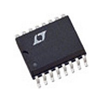
LT1054CSW#TRMPBF Linear Technology, LT1054CSW#TRMPBF Datasheet

LT1054CSW#TRMPBF
Specifications of LT1054CSW#TRMPBF
Available stocks
Related parts for LT1054CSW#TRMPBF
LT1054CSW#TRMPBF Summary of contents
Page 1
... External Shutdown External Oscillator Synchronization Can Be Paralleled ® Pin Compatible with the LTC 1044/LTC7660 U APPLICATIO S Voltage Inverter Voltage Regulator Negative Voltage Doubler Positive Voltage Doubler , LTC and LT are registered trademarks of Linear Technology Corporation. W BLOCK DIAGRA V REF 6 2.5V REFERENCE R + – 1 OSC ...
Page 2
LT1054/LT1054L BSOLUTE Supply Voltage (Note 2) LT1054 ................................................................ 16V LT1054L ................................................................ 7V Input Voltage Pin 1 ................................................. 0V V Pin 3 (S Package) ............................. 0V V Pin 7 ............................................. 0V V Pin 13 ...
Page 3
ELECTRICAL C HARA TERISTICS C temperature range, otherwise specifications are at T PARAMETER Supply Current Supply Voltage Range Voltage Loss (V – OUT Output Resistance Oscillator Frequency Reference Voltage Regulated Voltage Line Regulation Load Regulation Maximum Switch ...
Page 4
LT1054/LT1054L W U TYPICAL PERFOR A Shutdown Threshold 0.6 0.5 V PIN1 0.4 0.3 0.2 0.1 0 – 50 – 100 125 TEMPERATURE (˚C) LT1054 • TPC01 Supply Current in Shutdown 120 100 V = ...
Page 5
W U TYPICAL PERFOR A Regulated Output Voltage –4.7 –4.8 –4.9 –5.0 –5.1 –11.6 –11.8 –12.0 –12.2 –12.4 –12.6 – –25 TEMPERATURE (° PIN FUNCTIONS FB/SHDN (Pin 1): Feedback/Shutdown Pin. This pin has two functions. ...
Page 6
LT1054/LT1054L PIN FUNCTIONS from being pulled above the ground pin (Pin 3) during start-up. Any small, general purpose transistor such as 2N2222 or 2N2219 can be used. R provide enough base drive to the external transistor so ...
Page 7
PIN FUNCTIONS the oscillator frequency. During the time that C ing, the peak supply current will be approximately equal to 2.2 times the output current. During the time that C delivering charge to C the supply current ...
Page 8
LT1054/LT1054L U U APPLICATIONS INFORMATION R3 FB/SHDN CAP + GND TANTALUM CAP RESTART SHUTDOWN | | | | OUT OUT = + 1.21V REF – 40mV 2 ...
Page 9
U U APPLICATIONS INFORMATION where dV = peak-to-peak ripple and f = oscillator frequency. For output capacitors with significant ESR a second term must be added to account for the voltage step at the switch transitions. This step is approximately ...
Page 10
LT1054/LT1054L U TYPICAL APPLICATIONS Basic Voltage Inverter + FB/SHDN V + CAP OSC + LT1054 100 F GND V REF – CAP V OUT Negative Voltage Doubler + FB/SHDN V + CAP OSC + LT1054 V GND V IN REF ...
Page 11
U TYPICAL APPLICATIONS +V OUT OUT –V OUT V = LT1054 VOLTAGE LOSS FB/SHDN V + CAP OSC + LT1054 # GND V REF – CAP V OUT 10k INPUT ...
Page 12
LT1054/LT1054L U TYPICAL APPLICATIONS V IN 3.5V TO 5.5V 20k 1N914 1N914 1N914 + 3. OUT I = 50mA OUT(MAX) FB/SHDN CAP LT1054 #1 10 GND 10 F 1/2W + ...
Page 13
PACKAGE DESCRIPTION CORNER LEADS OPTION .045 – .068 (1.143 – 1.650) FULL LEAD OPTION .300 BSC (7.62 BSC) .008 – .018 (0.203 – 0.457) NOTE: LEAD DIMENSIONS APPLY TO SOLDER DIP/PLATE OR TIN PLATE LEADS U J8 Package 8-Lead CERDIP ...
Page 14
LT1054/LT1054L PACKAGE DESCRIPTION .300 – .325 (7.620 – 8.255) .008 – .015 (0.203 – 0.381) +.035 .325 –.015 +0.889 8.255 –0.381 NOTE: 1. DIMENSIONS ARE *THESE DIMENSIONS DO NOT INCLUDE MOLD FLASH OR PROTRUSIONS. MOLD FLASH OR PROTRUSIONS SHALL NOT ...
Page 15
... MOLD FLASH OR PROTRUSIONS SHALL NOT EXCEED .006" (0.15mm) Information furnished by Linear Technology Corporation is believed to be accurate and reliable. However, no responsibility is assumed for its use. Linear Technology Corporation makes no represen- tation that the interconnection of its circuits as described herein will not infringe on existing patent rights. ...
Page 16
... LTC3250/LTC3250-1.2/ Inductorless Step-Down DC/DC Converter LTC3250-1.5 LTC3251 500mA Spread Spectrum Inductorless Step-Down DC/DC Converter V LTC3252 Dual 250mA, Spread Spectrum Inductorless Step-Down DC/DC Converter ThinSOT is a trademark of Linear Technology Corporation. Linear Technology Corporation 16 1630 McCarthy Blvd., Milpitas, CA 95035-7417 (408) 432-1900 FAX: (408) 434-0507 N V ...


