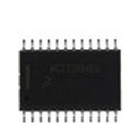
MCZ33991EG Freescale, MCZ33991EG Datasheet - Page 3

MCZ33991EG
Manufacturer Part Number
MCZ33991EG
Description
Manufacturer
Freescale
Datasheet
1.MCZ33991EG.pdf
(36 pages)
Specifications of MCZ33991EG
Operating Current
6mA
Operating Temperature Classification
Automotive
Package Type
SOIC W
Operating Supply Voltage (min)
4.5V
Operating Supply Voltage (typ)
5V
Operating Supply Voltage (max)
5.5V
Lead Free Status / RoHS Status
Compliant
Available stocks
Company
Part Number
Manufacturer
Quantity
Price
Part Number:
MCZ33991EG
Manufacturer:
FREESCALE
Quantity:
20 000
Analog Integrated Circuit Device Data
Freescale Semiconductor
Table 1. 33991 Pin Definitions
Pin Number
5 - 8
10
11
12
13
14
1
2
3
4
9
Pin Name
COS0+
SIN0+
COS0-
SIN0-
SCLK
GND
V
RTZ
SO
CS
SI
DD
H-Bridge Output. This is the output pin of a half bridge, designed to source or sink current. The H-Bridge
pins linearly drive the sine and cosine coils of two separate stepper motors to provide four-quadrant
operation.
H-Bridge Output. This is the output pin of a half bridge, designed to source or sink current. The H-Bridge
pins linearly drive the sine and cosine coils of two separate stepper motors to provide four-quadrant
operation.
H-Bridge Output. This is the output pin of a half bridge, designed to source or sink current. The H-Bridge
pins linearly drive the sine and cosine coils of two separate stepper motors to provide four-quadrant
operation.
H-Bridge Output. This is the output pin of a half bridge, designed to source or sink current. The H-Bridge
pins linearly drive the sine and cosine coils of two separate stepper motors to provide four-quadrant
operation.
Ground. These pins serve as the ground for the source of the low-side output transistors as well as the
logic portion of the device. They also help dissipate heat from the device.
Chip Select. This pin is connected to a chip select output of a LSI IC. This IC controls which device is
addressed by pulling the CS pin of the desire device low, enabling the SPI communication with the device,
while other devices on the serial link keep their serial outputs tri-stated. This input has an internal active
pull-up, requiring CMOS logic levels. This pin is also used to calibrate the internal clock.
Serial Clock. This pin is connected to the SCLK pin of the master device and acts as a bit clock for the
SPI port. It transitions on time per bit transferred at an operating frequency, fSPI, defined in the Coil Output
Timing Table. It is idle between command transfers. The pin is 50 percent duty cycle, with CMOS logic
levels. This signal is used to shift data to and from the device.
Serial Output. This pin is connected to the SPI Serial Data Input pin of the master device, or to the SI pin
of the next device in a daisy chain. This output will remain tri-stated unless the device is selected by a low
CS signal. The output signal generated will have CMOS logic levels and the output will transition on the
rising edges of SCLK. The serial output data provides status feedback and fault information for each output
and is returned MSB first when the device is addressed.
Serial Input. This pin is connected to the SPI Serial Data Output pin of the master device from which it
receives output command data. This input has an internal active pull down requiring CMOS logic levels.
The serial data transmitted on this line is a 16-bit control command sent MSB first, controlling the gauge
functions. The master ensures data is available on the falling edge of SCLK.
Multiplexed Output. This multiplexed output pin of the non-driven coil during an RTZ event.
Voltage. This SPI and logic power supply input will work with 5.0 V supplies.
COS0+
SIN0+
COS0
SCLK
SIN0
GND
GND
GND
GND
PIN CONNECTIONS
SO
CS
SI
2
3
4
5
6
7
8
9
10
11
12
1
24
23
22
21
20
19
18
17
16
15
14
13
Definitions
COS1+
COS1-
SIN1+
SIN1-
GND
GND
GND
GND
V
RST
V
RTZ
PWR
DD
PIN CONNECTIONS
33991
3


