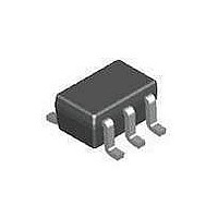
SIP32431DR3-T1GE3 Vishay, SIP32431DR3-T1GE3 Datasheet - Page 8

SIP32431DR3-T1GE3
Manufacturer Part Number
SIP32431DR3-T1GE3
Description
Power Switch ICs - Power Distribution 1A Slew Rate Ctrl Load Switch
Manufacturer
Vishay
Series
-r
Type
High Sider
Specifications of SIP32431DR3-T1GE3
On Resistance (max)
230 mOhms
Maximum Operating Temperature
+ 85 C
Minimum Operating Temperature
- 40 C
Package / Case
SC70-6
Maximum Power Dissipation
250 mW
Mounting Style
SMD/SMT
Number Of Switches
Single
Off Time (max)
10 us
On Time (max)
40 us
Supply Current
1 A
Supply Voltage (max)
5.5 V
Supply Voltage (min)
1.1 V
Switch Configuration
Single
Switch Current (typ)
1.2 A
Input Type
Non-Inverting
Number Of Outputs
1
On-state Resistance
147 mOhm
Current - Output / Channel
1A
Current - Peak Output
3A
Voltage - Supply
1.5 V ~ 5.5 V
Operating Temperature
-40°C ~ 85°C
Mounting Type
Surface Mount
Lead Free Status / RoHS Status
Supplier Unconfirmed
Available stocks
Company
Part Number
Manufacturer
Quantity
Price
SiP32431
Vishay Siliconix
DETAILED DESCRIPTION
The SiP32431 is a P-Channel MOSFET power switches
designed for high-side slew rate controlled load-switching
applications. Once turned on, the slew-rate control circuitry
is activated and current is ramped in a linear fashion until it
reaches the level required for the output load condition. This
is accomplished by first elevating the gate voltage of the
MOSFET up to its threshold voltage and then by linearly
increasing the gate voltage until the MOSFET becomes fully
enhanced. At this point, the gate voltage is then quickly
increased to the full input voltage to reduce R
MOSFET switch and minimize any associated power losses.
APPLICATION INFORMATION
Input Capacitor
While a bypass capacitor on the input is not required, a 1 µF
or larger capacitor for C
applications. The bypass capacitor should be placed as
physically close as possible to the SiP32431 to be effective
in minimizing transients on the input. Ceramic capacitors are
recommended over tantalum because of their ability to
withstand input current surges from low impedance sources
such as batteries in portable devices.
Output Capacitor
A 0.1 µF capacitor or larger across V
recommended to insure proper slew operation. C
increased without limit to accommodate any load transient
condition with only minimal affect on the SiP32431 turn on
slew rate time. There are no ESR or capacitor type
requirement.
Enable
The On/Off pin is compatible with both TTL and CMOS logic
voltage levels.
Protection Against Reverse Voltage Condition
The SiP32431 contains a body snatcher
connect the body to the Source (IN) when the device is
enable. In case where the device is disabled but the V
higher than the V
reverse bias the body diode to prevent the current from going
back to the input.
Thermal Considerations
The SiP32431 is designed to maintain a constant output load
current. Due to physical limitations of the layout and
assembly of the device the maximum switch current is 1.0 A,
as stated in the Absolute Maximum Ratings table. However,
another limiting characteristic for the safe operating load
current is the thermal power dissipation of the package. To
obtain the highest power dissipation (and a thermal
resistance of 170 °C/W) the power pad of the device should
be connected to a heat sink on the printed circuit board.
Vishay Siliconix maintains worldwide manufacturing capability. Products may be manufactured at one of several qualified locations. Reliability data for Silicon
Technology and Package Reliability represent a composite of all qualified locations. For related documents such as package/tape drawings, part marking, and
reliability data, see www.vishay.com/ppg?66597.
www.vishay.com
8
IN
, the n-type body is switched to OUT,
IN
is recommended in almost all
OUT
that normally
DS(ON)
and GND is
OUT
may be
OUT
of the
is
The maximum power dissipation in any application is
dependant
T
for the TDFN4 1.2 mm x 1.6 mm package, θ
and the ambient temperature, T
expressed as:
P
It then follows that, assuming an ambient temperature of
70 °C, the maximum power dissipation will be limited to about
324 mW.
So long as the load current is below the 1.0 A limit, the
maximum continuous switch current becomes a function two
things: the package power dissipation and the R
ambient temperature.
As an example let us calculate the worst case maximum load
current at T
occurs at an input voltage of 1.5 V and is equal to 520 mΩ.
The R
using the following formula
R
Where T
we have
R
= 597 mΩ
The maximum current limit is then determined by
I
which in case is 0.74 A. Under the stated input voltage
condition, if the 0.74 A current limit is exceeded the internal
die temperature will rise and eventually, possibly damage the
device.
LOAD
J(MAX)
DS(ON)
DS(ON)
(max.)
(max.)
DS(ON
= 125 °C, the junction-to-ambient thermal resistance
(at 70 °C) = R
(at 70 °C) = 520 mΩ x (1 + 0.0033 x (70 °C - 25 °C))
C
=
is 3300 ppm/°C. Continuing with the calculation
) at 70 °C can be extrapolated from this data
<
T
A
on
J
= 70 °C. The worst case R
(max.)
R
θ
P
J
the
DS
(max.)
-
A
(
ON
-
DS(ON)
T
maximum
)
A
=
(at 25 °C) x (1 + T
A
125
, which may be formulaically
S10-1225-Rev. A, 24-May-10
170
Document Number: 66597
-
junction
T
A
DS(ON)
J-A
temperature,
DS(ON)
= 170 °C/W,
C
x ΔT)
at 25 °C
at the


