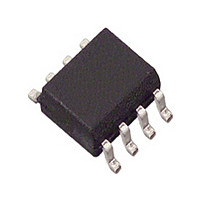
ADP3820AR-4.2-REEL Analog Devices Inc, ADP3820AR-4.2-REEL Datasheet - Page 7

ADP3820AR-4.2-REEL
Manufacturer Part Number
ADP3820AR-4.2-REEL
Description
Manufacturer
Analog Devices Inc
Type
Battery Chargerr
Datasheet
1.ADP3820AR-4.2-REEL.pdf
(8 pages)
Specifications of ADP3820AR-4.2-REEL
Battery Type
Li-Ion
Output Current
1mA
Output Voltage
4.2V
Operating Supply Voltage (min)
4.5V
Operating Supply Voltage (max)
15V
Operating Temp Range
-20C to 85C
Package Type
SOIC N
Mounting
Surface Mount
Pin Count
8
Operating Temperature Classification
Commercial
Lead Free Status / RoHS Status
Not Compliant
The current sense resistor for this application:
FET Selection
The type and size of the pass transistor are determined by the
threshold voltage, input-output voltage differential and load
current. The selected PMOS must satisfy the physical and ther-
mal design requirements. To ensure that the maximum V
provided by the controller will turn on the FET at worst case
conditions, (i.e., temperature and manufacturing tolerances) the
maximum available V
calculated as follows:
where
I
R
V
For example:
If V
If V
used.
The difference between V
voltage drop due to the sense resistor plus the ON-resistance
of the FET at the maximum charge current. The selected
MOSFET must satisfy these criteria; otherwise, a different pass
device should be used.
The maximum R
and Drain-to-Source voltage (V
From the Drain-to Source current vs. Drain-to-Source voltage
vs. gate drive graph off the MOSFET data sheet, it can be de-
termined if the above calculated R
indicates. However, the value read from the MOSFET data
sheet graph must be adjusted based on the junction temperature
of the MOSFET. This adjustment factor can be obtained from
the normalized R
MOSFET data sheet.
External Capacitors
The ADP3820 is stable with or without a battery load, and
virtually any good quality output filter capacitors can be used
(anyCAP™), independent of the capacitor’s minimum ESR
(Effective Series Resistance) value. The actual value of the
capacitor and its associated ESR depends on the g
tance of the external PMOS device. A 10 F tantalum or alumi-
num electrolytic capacitor at the output is sufficient to ensure
stability for up to a 10 A output current.
Shutdown Mode
Applying a TTL high signal to the SD pin or tying it to the
input pin will enable the output. Pulling this pin low or tying
it to ground will disable the output. In shutdown mode, the
controller’s quiescent current is reduced to less than 1 A.
anyCAP is a trademark of Analog Devices, Inc.
REV. A
OUTMAX
S
BE
GS
GS
< 5 V, logic level FET should be considered.
> 5 V, either logic level or standard MOSFET can be
= Maximum Output Current
= Current Sense Resistor
~ 0.7 V (Room Temperature)
~ 0.5 V (Hot)
~ 0.9 V (Cold)
V
GS
V
DS
= 5 V – 0.7 V – 1 A
R
V
V
DS(ON)
DS(ON)
S
= V
GS
IN
= V
= V
= 5 V, and I
R
IN
GS
DS(ON)
S
required at the available gate drive (V
/I
vs. junction temperature graph in the
– V
must be determined. Maximum V
IN
O
IN
– V
= 0.05/0.5 = 100 m
O
and V
= V
= 5 V – 4.2 V = 0.8 V
BE
DS
DS
– I
OUTMAX
) is:
O
DS(ON)
/I
OUTMAX
(V
OUTMAX
50 m = 4.25 V
DS
is higher than the graph
) must exceed the
= 1 A,
R
S
m
and capaci-
GS
GS
DR
is
)
–7–
Gate-to-Source Clamp
A 6 V gate-to-source voltage clamp is provided by the ADP3820 to
protect most MOSFET gates in the event the V
and the output is suddenly shorted to ground. This allows use of
the new, low R
Short Circuit Protection
The power FET is protected during short circuit conditions
with a foldback type of current limiting that significantly re-
duces the current. See Figure 13 for foldback current limit
information.
Current Sense Resistor
Current limit is achieved by setting an appropriate current sense
resistor (R
limit sense resistor, R
derating is advised to select the power dissipation rating of the
resistor.
The simplest and cheapest sense resistor for high current appli-
cations, (i.e., Figure 1) is a PCB trace. However, the tempera-
ture dependence of the copper trace and the thickness tolerances of
the trace must be considered in the design. The resistivity of
copper has a positive temperature coefficient of +0.39%/ C.
Copper’s Tempco, in conjunction with the proportional-to-
absolute temperature ( 0.3%) current limit voltage, can provide
an accurate current limit. Table I provides the typical resistance
values for PCB copper traces. Alternately, an appropriate sense
resistor, such as surface mount sense resistors, available from
KRL, can be used.
Conductor
Thickness
1/2oz/ft
(18 m)
1oz/ft
(35 m)
2oz/ft
(70 m)
3oz/ft
(106 m)
2
2
2
2
Table I. Printed Circuit Copper Resistance
S
) across the current limit threshold voltage. Current
DS(ON)
S
MOSFETs.
, is calculated as shown above. Proper
Conductor
Width/Inch
0.025
0.050
0.100
0.200
0.500
0.025
0.050
0.100
0.200
0.500
0.025
0.050
0.100
0.200
0.500
0.025
0.050
0.100
0.200
0.500
ADP3820
IN
Resistance
m /In
39.3
19.7
9.83
4.91
1.97
19.7
9.83
4.91
2.46
0.98
9.83
4.91
2.46
1.23
0.49
6.5
3.25
1.63
0.81
0.325
> V
GS
allowed


