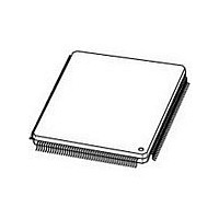
LH79525N0Q100A1 Sharp Electronics, LH79525N0Q100A1 Datasheet - Page 15

LH79525N0Q100A1
Manufacturer Part Number
LH79525N0Q100A1
Description
Manufacturer
Sharp Electronics
Datasheet
1.LH79525N0Q100A1.pdf
(64 pages)
Specifications of LH79525N0Q100A1
Operating Temperature (min)
-40C
Operating Temperature (max)
85C
Applications
Embedded Control
Processing Unit
Microcontroller
Operating Supply Voltage (min)
1.7/3V
Operating Supply Voltage (typ)
1.8/3.3V
Operating Supply Voltage (max)
1.9/3.6V
Package Type
LQFP
Screening Level
Industrial
Pin Count
176
Mounting
Surface Mount
Rad Hardened
No
Lead Free Status / RoHS Status
Compliant
Available stocks
Company
Part Number
Manufacturer
Quantity
Price
Company:
Part Number:
LH79525N0Q100A1
Manufacturer:
FREESCALE
Quantity:
101
Company:
Part Number:
LH79525N0Q100A1,55
Manufacturer:
NXP Semiconductors
Quantity:
10 000
System-on-Chip
Product data sheet
PIN NO.
141
139
138
137
136
134
133
120
153
151
149
147
146
145
143
142
162
161
159
158
157
156
155
154
171
170
169
167
166
165
164
53
52
90
89
88
87
85
84
83
82
PC6/A22/nFWE
PC7/A23/nFRE
PD0/D8
PD1/D9
PD2/D10
PD3/D11
PD4/D12
PD5/D13
PD6/D14
PD7/D15
PE0/LCDLP/
LCDHRLP
PE1/LCDDCLK
PE2/LCDPS
PE3/LCDCLS
PE4/LCDDSPLEN/
LCDREV
PE5/LCDVDDEN
PE6LCDVEEN/
LCDMOD
PE7/nWAIT/nDEOT
PF0/LCDVD6
PF1/LCDVD7
PF2/LCDVD8
PF3/LCDVD9
PF4/LCDVD10
PF5/LCDVD11
PF6/LCDEN/
LCDSPL
PF7/LCDFP/
LCDSPS
PG0/ETHERTXEN
PG1/ETHERTXCLK
PG2/LCDVD0
PG3/LCDVD1
PG4/LCDVD2
PG5/LCDVD3
PG6/LCDVD4
PG7/LCDVD5
PH0/ETHERRX3
PH1/ETHERRXDV
PH2/ETHERRXCLK
PH3/ETHERTXER
PH4/ETHERTX0
PH5/ETHERTX1
PH6/ETHERTX2
SIGNAL NAME
TYPE
I/O
I/O
I/O
I/O
I/O
I/O
I/O
I/O
I/O
I/O
I/O
I/O
I/O
I/O
I/O
I/O
I/O
I/O
I/O
I/O
I/O
I/O
I/O
I/O
I/O
I/O
I/O
I/O
I/O
I/O
I/O
I/O
I/O
I/O
I/O
I/O
I/O
I/O
I/O
I/O
I/O
Table 5. LH79525 Pin Descriptions (Cont’d)
General Purpose I/O Signal — Port C6; multiplexed with Address A22 and NAND
Flash Write Enable
General Purpose I/O Signal — Port C7; multiplexed with Address A23 and NAND
Flash Read Enable
General Purpose I/O Signal — Port D0; multiplexed with Data D8
General Purpose I/O Signal — Port D1; multiplexed with Data D9
General Purpose I/O Signal — Port D2; multiplexed with Data D10
General Purpose I/O Signal — Port D3; multiplexed with Data D11
General Purpose I/O Signal — Port D4; multiplexed with Data D12
General Purpose I/O Signal — Port D5; multiplexed with Data D13
General Purpose I/O Signal — Port D6; multiplexed with Data D14
General Purpose I/O Signal — Port D7; multiplexed with Data D15
General Purpose I/O Signals — Port E0; multiplexed with LCD Line Pulse and
AD-TFT/HR-TFT Line Pulse
General Purpose I/O Signals — Port E1; multiplexed with LCD Data Clock
General Purpose I/O Signals — Port E2; multiplexed with LCD Power Save
General Purpose I/O Signals — Port E3; multiplexed with LCD Row Driver Clock
General Purpose I/O Signals — Port E4; multiplexed with LCD Panel Power
Enable and LCD Reverse
General Purpose I/O Signals — Port E5; multiplexed with LCD VDD Enable
General Purpose I/O Signals — Port E6; multiplexed with LCD Analog Power
Enable and MOD
General Purpose I/O Signals — Port E7; multiplexed with nWAIT and DMA
End of Transfer
General Purpose I/O Signals — Port F0; multiplexed with LCD Video Data bit 6
General Purpose I/O Signals — Port F1; multiplexed with LCD Video Data bit 7
General Purpose I/O Signals — Port F2; multiplexed with LCD Video Data bit 8
General Purpose I/O Signals — Port F3; multiplexed with LCD Video Data bit 9
General Purpose I/O Signals — Port F4; multiplexed with LCD Video Data bit 10
General Purpose I/O Signals — Port F5; multiplexed with LCD Video Data bit 11
General Purpose I/O Signals — Port F6; multiplexed with LCD Start Pulse Left
General Purpose I/O Signals — Port F7; multiplexed with LCD Row Driver Counter reset
General Purpose I/O Signals — Port G0; multiplexed with Ethernet Transmit Enable
General Purpose I/O Signals — Port G1; multiplexed with Ethernet Clock
General Purpose I/O Signals — Port G2; multiplexed with LCD Video Data bit 0
General Purpose I/O Signals — Port G3; multiplexed with LCD Video Data bit 1
General Purpose I/O Signals — Port G4; multiplexed with LCD Video Data bit 2
General Purpose I/O Signals — Port G5; multiplexed with LCD Video Data bit 3
General Purpose I/O Signals — Port G6; multiplexed with LCD Video Data bit 4
General Purpose I/O Signals — Port G7; multiplexed with LCD Video Data bit 5
General Purpose I/O Signals — Port H0; multiplexed with Ethernet Receive Channel 3
General Purpose I/O Signals — Port H1; multiplexed with Ethernet Data Valid
General Purpose I/O Signals — Port H2; multiplexed with Ethernet Receive Clock
General Purpose I/O Signals — Port H3; multiplexed with Ethernet Transmit Error
General Purpose I/O Signals — Port H4; multiplexed with Ethernet Transmit Channel 0
General Purpose I/O Signals — Port H5; multiplexed with Ethernet Transmit Channel 1
General Purpose I/O Signals — Port H6; multiplexed with Ethernet Transmit Channel 2
Rev. 02 — 17 March 2009
NXP Semiconductors
DESCRIPTION
LH79524/LH79525
15


