IDT74CBTLV3383PG IDT, Integrated Device Technology Inc, IDT74CBTLV3383PG Datasheet - Page 2
IDT74CBTLV3383PG
Manufacturer Part Number
IDT74CBTLV3383PG
Description
Manufacturer
IDT, Integrated Device Technology Inc
Datasheet
1.IDT74CBTLV3383PG.pdf
(5 pages)
Specifications of IDT74CBTLV3383PG
Lead Free Status / RoHS Status
Not Compliant


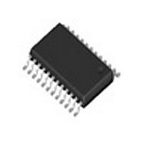
PIN CONFIGURATION
OPERATING CHARACTERISTICS, T
NOTE:
1. All unused control inputs of the device must be held at V
IDT74CBTLV3383
LOW-VOLTAGE 10-BIT BUS-EXCHANGE SWITCH
Symbol
V
V
V
T
CC
IH
IL
A
GND
Parameter
Supply Voltage
High-Level Control Input Voltage
Low-Level Control Input Voltage
Operating Free-Air Temperature
1
1
2
2
3
1
1
2
2
3
BE
A
B
A
A
B
A
B
A
B
B
2
2
2
1
1
1
1
1
2
1
SSOP/ QSOP/ TSSOP
12
10
11
1
2
4
3
5
6
7
8
9
TOP VIEW
13
24
23
22
21
20
19
18
17
16
15
14
CC
or GND to ensure proper device operation.
V
5
5
5
5
4
4
4
3
BX
4
3
B
A
B
A
B
B
A
A
B
A
CC
2
2
2
1
1
1
2
1
2
2
Test Conditions
V
V
V
V
CC
CC
CC
CC
A
= 2.3V to 2.7V
= 2.7V to 3.6V
= 2.3V to 2.7V
= 2.7V to 3.6V
= 25°C
2
NOTE:
1. Stresses greater than those listed under ABSOLUTE MAXIMUM RATINGS may cause
FUNCTION TABLE
ABSOLUTE MAXIMUM RATINGS
NOTE:
1. H = HIGH Voltage Level
Symbol
V
V
I
T
IK
permanent damage to the device. This is a stress rating only and functional operation
of the device at these or any other conditions above those indicated in the operational
sections of this specification is not implied. Exposure to absolute maximum rating
conditions for extended periods may affect reliability.
STG
X = Don’t Care
L = LOW Voltage Level
Z = High Impedance
CC
I
(1)
BE
H
L
L
SupplyVoltage Range
Input Voltage Range
Continuous Channel Current
Input Clamp Current, V
Storage Temperature
Input
Min.
−40
2.3
1.7
Description
—
—
BX
2
H
X
L
INDUSTRIAL TEMPERATURE RANGE
I/O
(1)
< 0
1
1
1
A
B
B
Max.
1
1
2
3.6
0.7
0.8
—
—
85
Z
-
-
-
5
5
5
A
B
B
Inputs/Outputs
1
1
2
–0.5 to +4.6
–0.5 to +4.6
–65 to +150
Max
128
–50
1
1
1
A
B
B
(1)
2
1
Unit
2
°C
Z
V
V
V
-
-
-
5
5
5
A
B
B
2
2
1
Unit
mA
mA
° C
V
V
Related parts for IDT74CBTLV3383PG
Image
Part Number
Description
Manufacturer
Datasheet
Request
R

Part Number:
Description:
TRANSLATION DEVICE DPI 80-PQFP
Manufacturer:
IDT, Integrated Device Technology Inc
Datasheet:
Part Number:
Description:
IDT PART
Manufacturer:
IDT, Integrated Device Technology Inc
Datasheet:
Part Number:
Description:
IC LIU T1/E1/J1 OCTAL 256PBGA
Manufacturer:
IDT, Integrated Device Technology Inc
Datasheet:

Part Number:
Description:
IC FREQ TIMING GENERATOR 28TSSOP
Manufacturer:
IDT, Integrated Device Technology Inc
Datasheet:
Part Number:
Description:
IC CLK DVR PLL 1:10 40VFQFPN
Manufacturer:
IDT, Integrated Device Technology Inc
Datasheet:
Part Number:
Description:
IC CLK FANOUT BUFFER 1:18 32LQFP
Manufacturer:
IDT, Integrated Device Technology Inc
Datasheet:
Part Number:
Description:
IC CLK FANOUT BUFFER 1:18 32LQFP
Manufacturer:
IDT, Integrated Device Technology Inc
Datasheet:
Part Number:
Description:
IC CK505 VREG/RES 56TSSOP
Manufacturer:
IDT, Integrated Device Technology Inc
Datasheet:

Part Number:
Description:
IC SDRAM CLK DVR 1:10 48-TSSOP
Manufacturer:
IDT, Integrated Device Technology Inc
Datasheet:

Part Number:
Description:
IC CLK DVR PLL 1:10 48TSSOP
Manufacturer:
IDT, Integrated Device Technology Inc
Datasheet:
Part Number:
Description:
IC FLEXPC CLK PROGR P4 56-TSSOP
Manufacturer:
IDT, Integrated Device Technology Inc
Datasheet:
Part Number:
Description:
IC FLEXPC CLK PROGR P4 56-TSSOP
Manufacturer:
IDT, Integrated Device Technology Inc
Datasheet:
Part Number:
Description:
IC FLEXPC CLK PROGR P4 56-SSOP
Manufacturer:
IDT, Integrated Device Technology Inc
Datasheet:

Part Number:
Description:
IC PLL CLK DRIVER 2.5V 28-TSSOP
Manufacturer:
IDT, Integrated Device Technology Inc
Datasheet:
Part Number:
Description:
IC CLOCK DRIVER 2.5V 24-TSSOP
Manufacturer:
IDT, Integrated Device Technology Inc
Datasheet: