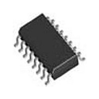
SM16LC05-LF ProTek Devices, SM16LC05-LF Datasheet - Page 4

SM16LC05-LF
Manufacturer Part Number
SM16LC05-LF
Description
Manufacturer
ProTek Devices
Datasheet
1.SM16LC05-LF.pdf
(5 pages)
Specifications of SM16LC05-LF
Number Of Elements
8
Polarity
Uni-Directional
Package Type
SOIC
Operating Temperature Classification
Military
Reverse Breakdown Voltage
6V
Clamping Voltage
24V
Reverse Stand-off Voltage
5V
Leakage Current (max)
20uA
Peak Pulse Current
42A
Peak Pulse Power Dissipation
500W
Test Current (it)
1mA
Operating Temp Range
-55C to 150C
Mounting
Surface Mount
Pin Count
16
Lead Free Status / RoHS Status
Compliant
APPLICATION NOTE
The SM16LC & SM16LCxxC Series are TVS arrays designed to protect I/O or data lines from the damaging effects of ESD, EFT and other types of
surges. This product series provides both unidiretional and bidirectional protection, with a surge capability of 500 Watts P
waveform and ESD protection > 40kV.
BIDIRECTIONAL COMMON-MODE CONFIGURATION (Figure 1)
Ideal for RS-485 applications, the SM16LCxxC Series provides up to eight (8) lines of protection in a common-mode configuration as depicted in
Figure 1. This low capacitance series allows the transceiver or telecommunications circuit to operate safely without significant signal distortion.
Circuit connectivity is as follows:
✔
✔
✔
✔
✔
✔
✔
✔
✔
CIRCUIT BOARD LAYOUT RECOMMENDATIONS
Circuit board layout is critical for Electromagnetic Compatibility
(EMC) protection. The following guidelines are recommended:
✔
✔
✔
✔
✔
05051.R12 4/08
Lines 1 is connected to Pin 9.
Line 2 is connected to Pin 10.
Line 3 is connected to Pin 11.
Line 4 is connected to Pin 12.
Line 5 is connected to Pin 13.
Line 6 is connected to Pin 14.
Line 7 is connected to Pin 15.
Line 8 is connected to Pin 16.
Pins 1-8 are connected to ground.
The protection device should be placed near the input
terminals or connectors, the device will divert the
transient current immediately before it can be coupled
into the nearby traces.
The path length between the TVS device and the
protected line should be minimized.
All conductive loops including power and ground loops
should be minimized.
The transient current return path to ground should be
kept as short as possible to reduce parasitic inductance.
Ground planes should be used whenever possible. For
multilayer PCBs, use ground vias.
4
TRANSCEIVER
D
D
R
R
Figure 1. Birectional Common-Mode Protection
16
LINE 1
LINE 2
LINE 3
LINE 4
LINE 5
LINE 6
LINE 7
LINE 8
1
15
2
14
3
13
4
12
SM16LC36C
5
PP
per line for an 8/20µs
SM16LC03
11
6
www.protekdevices.com
10
7
thru
9
8


