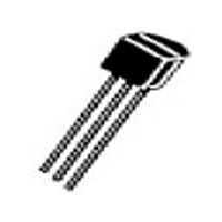
MPF4393 ON Semiconductor, MPF4393 Datasheet - Page 4

MPF4393
Manufacturer Part Number
MPF4393
Description
Manufacturer
ON Semiconductor
Datasheet
1.MPF4393.pdf
(6 pages)
Specifications of MPF4393
Channel Type
N
Configuration
Single
Gate-source Voltage (max)
30V
Drain-gate Voltage (max)
30V
Drain-source Volt (max)
30V
Operating Temperature (max)
150C
Operating Temperature Classification
Military
Mounting
Through Hole
Pin Count
3
Package Type
TO-92
Lead Free Status / RoHS Status
Not Compliant
Available stocks
Company
Part Number
Manufacturer
Quantity
Price
Company:
Part Number:
MPF4393RL1
Manufacturer:
MOT
Quantity:
500
PULSE WIDTH = 2.0 ms
DUTY CYCLE ≤ 2.0%
R
50 W
200
160
120
7.0
5.0
3.0
2.0
20
10
80
40
GEN
V
0
GEN
0.5
0
I
= 10
mA
Figure 5. Switching Time Test Circuit
Figure 6. Typical Forward Transfer Admittance
DSS
INPUT PULSE
0.7
INPUT
t
r
Figure 8. Effect of Gate−Source Voltage
t
≤ 0.25 ns
f
1.0
MPF4393
≤ 0.5 ns
25
mA
1.0
50
W
V
On Drain−Source Resistance
SET V
GS
50 mA
2.0
R
, GATE−SOURCE VOLTAGE (VOLTS)
K
2.0
I
DS(off)
R
D
R
, DRAIN CURRENT (mA)
GG
T
V
channel
D
DS
3.0
75 mA 100 mA
3.0
′ = R
& R
= 10 V
= 15 V
R
R
V
D
GG
GG
D
K
+ R
= 25°C
(R
4.0
5.0
T
T
+ 50)
+ 50
MPF4392
7.0
V
R
5.0
DD
D
10
125 mA
T
50
W
R
channel
6.0
T
MPF4392, MPF4393
20
= 25°C
http://onsemi.com
7.0
30
OUTPUT
8.0
50
4
The switching characteristics shown above were measured using a
test circuit similar to Figure 5. At the beginning of the switching
interval, the gate voltage is at Gate Supply Voltage (−V
Drain−Source Voltage (V
Voltage (V
Capacitance (C
V
discharges through the series combination of R
must discharge to V
parallel combination of effective load impedance (R′
Drain−Source Resistance (r
flow is reversed.
resistance r
discharges, V
discharges through r
the situation is reversed with r
1) R
cascaded stages where the driving source impedance is normally the
load impedance of the previous stage, and 2) R
impedance) the driving source impedance is that of the generator.
GG
During the turn−on interval, Gate−Source Capacitance (C
Predicting turn−on time is somewhat difficult as the channel
The above switching curves show two impedance conditions:
K
7.0
5.0
3.0
2.0
1.5
1.0
1.0
0.8
0.6
0.4
2.0
1.6
1.4
1.2
1.8
15
10
+ V
0.03
is equal to R
−70
DS
0.05
DD
ds
.
) due to the voltage divider. Thus Reverse Transfer
is a function of the gate−source voltage. While C
GS
−40
I
V
D
rss
GS
T
(C
Drain−Source On−State Resistance
Figure 9. Effect of Temperature On
= 1.0 mA
channel
0.1
) or Gate−Drain Capacitance (C
approaches zero and r
ds
= 0
Figure 7. Typical Capacitance
T
ds
D
IS NEGLIGIBLE)
DS(on)
channel
′ which simulates the switching behavior of
−10
, turn−on time is non−linear. During turn−off,
V
= 25°C
R
, REVERSE VOLTAGE (VOLTS)
DS
, CHANNEL TEMPERATURE (°C)
0.3
through R
) is slightly lower than Drain Supply
ds
20
NOTE 1
). During the turn−off, this charge
ds
0.5
increasing as C
1.0
50
G
C
C
and R
gs
gd
ds
80
decreases. Since C
3.0
K
gd
in series with the
Gen
5.0
gd
110
charges.
) is charged to
and R
K
10
= 0 (low
GG
140
D
K
). The
) and
. C
gs
gd
gd
gs
170
)
30


