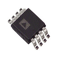
AD8315ARM-REEL Analog Devices Inc, AD8315ARM-REEL Datasheet - Page 13

AD8315ARM-REEL
Manufacturer Part Number
AD8315ARM-REEL
Description
Manufacturer
Analog Devices Inc
Datasheet
1.AD8315ARM-REEL.pdf
(24 pages)
Specifications of AD8315ARM-REEL
Operating Supply Voltage (typ)
3.3/5V
Operating Supply Voltage (min)
2.7V
Operating Supply Voltage (max)
5.5V
Operating Temp Range
-30C to 85C
Operating Temperature Classification
Commercial
Mounting
Surface Mount
Pin Count
8
Lead Free Status / RoHS Status
Not Compliant
Available stocks
Company
Part Number
Manufacturer
Quantity
Price
Company:
Part Number:
AD8315ARM-REEL
Manufacturer:
TOSHIBA
Quantity:
3 000
Part Number:
AD8315ARM-REEL
Manufacturer:
ADI/亚德诺
Quantity:
20 000
Company:
Part Number:
AD8315ARM-REEL7
Manufacturer:
AD
Quantity:
10 977
Company:
Part Number:
AD8315ARM-REEL7
Manufacturer:
microsemi
Quantity:
11 000
Part Number:
AD8315ARM-REEL7
Manufacturer:
ADI/亚德诺
Quantity:
20 000
The intercept need not correspond to a physically realizable
part of the signal range for the log amp. Therefore, the specified
intercept is −70 dBV, at 0.1 GHz, whereas the smallest input for
accurate measurement (a +1 dB error, see Table 2) at this
frequency is higher, being about −58 dBV. At 2.5 GHz, the
+1 dB error point shifts to −64 dBV. This positioning of the
intercept is deliberate and ensures that the V
the capabilities of certain DACs, whose outputs cannot swing
below 200 mV. Figure 32 shows the 100 MHz response of the
AD8315; the vertical axis does not represent the output (at pin
VAPC) but the value required at the power control pin, VSET,
to null the control loop.
CONTROLLER-MODE LOG AMPS
The AD8315 combines the two key functions required for the
measurement and control of the power level over a moderately
wide dynamic range. First, it provides the amplification needed
to respond to small signals in a chain of four amplifier/limiter
cells (see Figure 31), each having a small signal gain of 10 dB
and a bandwidth of approximately 3.5 GHz. At the output of
each of these amplifier stages is a full-wave rectifier, essentially a
square law detector cell that converts the RF signal voltages to a
fluctuating current having an average value that increases with
signal level. A further passive detector stage is added before the
first stage. These five detectors are separated by 10 dB, spanning
some 50 dB of dynamic range. Their outputs are each in the
form of a differential current, making summation a simple
matter. It is readily shown that the summed output can closely
approximate a logarithmic function. The overall accuracy at the
extremes of this total range, viewed as the deviation from an
ideal logarithmic response, that is, the log conformance error,
can be judged by referring to Figure 6, which shows that errors
across the central 40 dB are moderate. Other performance
curves show how conformance to an ideal logarithmic function
varies with supply voltage, temperature, and frequency.
1.5
1.0
0.5
–67dBm
–80dBV
100µV
0
–70dBV
Figure 32. Basic Calibration of the AD8315 at 0.1 GHz
–47dBm
–60dBV
1mV
IDEAL
0.288V @ –58dBV
V
IN
, dBV
–27dBm
–40dBV
10mV
IN
, P
1.416V @ –11dBV
IN
ACTUAL
–20dBV
100mV
–7dBm
SET
+13dBm (RE 50Ω)
voltage is within
1V (RMS)
0dBV
Rev. C | Page 13 of 24
In a device intended for measurement applications, this current
would then be converted to an equivalent voltage, to provide the
log (V
the AD8315 differs from standard practice in that its output
needs to be a low noise control voltage for an RF power amplifier
not a direct measure of the input level. Furthermore, it is highly
desirable that this voltage be proportional to the time integral of
the error between the actual input V
(applied to Pin 3, VSET) that defines the setpoint, that is, a
target value for the power level, typically generated by a DAC.
This is achieved by converting the difference between the sum
of the detector outputs (still in current form) and an internally
generated current proportional to V
current-mode signal. This, in turn, is converted to a voltage (at
Pin 4, FLTR, the low-pass filter capacitor node) to provide a
close approximation to an exact integration of the error between
the power present in the termination at the input of the AD8315
and the setpoint voltage. Finally, the voltage developed across
the ground-referenced filter capacitor C
special low noise amplifier of low voltage gain (×1.35) and
presented at Pin 7 (VAPC) for use as the control voltage for the
RF power amplifier. This buffer can provide rail-to-rail swings
and can drive a substantial load current, including large
capacitors. Note that the RF power amplifier is assumed to have
a positive slope with RF power increasing monotonically with
an increasing APC control voltage.
CONTROL LOOP DYNAMICS
To understand how the AD8315 behaves in a complete control
loop, an expression for the current in the integration capacitor
as a function of the input V
be developed (see Figure 33).
RFIN
V
1
SET
3
IN
) function shown in Equation 1. However, the design of
V
V
SET
IN
I
DET
Figure 33. Behavioral Model of the AD8315
RF DETECTION
LOGARITHMIC
INTERFACE
= I
SETPOINT
SUBSYSTEM
SLP
log
10
(V
IN
/V
I
IN
SET
Z
I
)
DET
and the setpoint voltage V
= V
SET
I
ERR
/4.15kΩ
SET
IN
FLTR
and the dc voltage V
to a single-sided,
4
FLT
C
FLT
is buffered by a
×1.35
AD8315
VAPC
7
SET
must
SET


