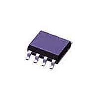
HV311LG Supertex, HV311LG Datasheet - Page 4

HV311LG
Manufacturer Part Number
HV311LG
Description
Hot Swap & Power Distribution Active Low
Manufacturer
Supertex
Specifications of HV311LG
Package Type
SOIC N
Operating Temperature (min)
-40C
Operating Temperature (max)
85C
Operating Temperature Classification
Industrial
Product Depth (mm)
3.9mm
Product Length (mm)
4.9mm
Mounting
Surface Mount
Pin Count
8
Operating Temperature Range
- 40 C to + 125 C
Mounting Style
SMD/SMT
Package / Case
SOIC-8
Lead Free Status / RoHS Status
Not Compliant
Available stocks
Company
Part Number
Manufacturer
Quantity
Price
Part Number:
HV311LG-M908
Manufacturer:
SUPERTEX
Quantity:
20 000
Functional Block Diagram
Functional Description
The HV301 provides control over the power supply cur-
rent on systems where circuit cards are inserted into live
backplanes. Such systems can frequently be found in the
telecom, data networking and computing industry. The de-
vice provides means of limiting the power supply current af-
ter contact with the live backplane is made, thereby protect-
ing card and backplane connectors and reducing the voltage
disturbance on the backplane’s power supply. Additional
protection is provided in the form of a circuit breaker function
and a start-up time limiter, both for protection of the external
MOSFET and the system as a whole.
Start-up Sequence
After first contact is made with the backplane, the HV301
tries to establish an internal bias supply of 10V. During this
time, GATE, PWRGD and RAMP are positively held low by
circuitry that can operate with partial supply voltage.
When the internal bias supply is in regulation, the undervoltage
(UV) and overvoltage (OV) comparators start monitoring the
external power supply. External resistor dividers at UV and
RAMP
UV
OV
~9.8V
SENSE
V
BG
Transconductor
Clamp Mechanism
gm
●
C
C
C
10µA
1235 Bordeaux Drive, Sunnyvale, CA 94089
5k
Logic
D
S
A
B
E
L
I
4
V
OV pin set the window for normal operating supply voltage.
These may be two individual dividers, or a single divider with
two taps, as shown in the application diagrams.
Once the power supply voltage is within normal operating
range, a 10μA internal source turns on to charge an external
capacitor at the RAMP pin. The voltage at the GATE output
follows the RAMP pin voltage with an offset of about 2.5V for
control of the external MOSFET.
Power supply current starts to flow once the GATE voltage
reaches the MOSFET threshold voltage, which is typically
in the 2.0 to 4.0V range. The current sense amplifier at the
SENSE pin reduces the RAMP charging current in propor-
tion to the supply current, thereby slowing the voltage rise
at RAMP, and thus the rise of the GATE voltage. At a sense
voltage of 50mV the RAMP current is reduced to zero, and
the RAMP and GATE voltages stop rising, thereby prevent-
ing a further rise in the power supply current.
U
H
G
H
EE
P
L
L
I
UVLO
Regulator & POR
2V
Transconductor
BG
●
Tel: 408-222-8888
V
1 : 2
REG
5kΩ
mirror
●
PWRGD
VDD
www.supertex.com
HV301
GATE


