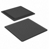
XC3SD3400A-5FGG676C Xilinx Inc, XC3SD3400A-5FGG676C Datasheet - Page 3

XC3SD3400A-5FGG676C
Manufacturer Part Number
XC3SD3400A-5FGG676C
Description
FPGA Spartan®-3A Family 3.4M Gates 53712 Cells 770MHz 90nm Technology 1.2V 676-Pin FBGA
Manufacturer
Xilinx Inc
Series
Spartan™-3A DSPr
Datasheets
1.XC3S50A-4VQG100C.pdf
(7 pages)
2.XC3SD3400A-4FGG676C.pdf
(4 pages)
3.XC3SD3400A-4FGG676C.pdf
(101 pages)
Specifications of XC3SD3400A-5FGG676C
Package
676FBGA
Family Name
Spartan®-3A
Device Logic Units
53712
Device System Gates
3400000
Maximum Internal Frequency
770 MHz
Typical Operating Supply Voltage
1.2 V
Maximum Number Of User I/os
469
Ram Bits
2322432
Number Of Logic Elements/cells
53712
Number Of Labs/clbs
5968
Total Ram Bits
2322432
Number Of I /o
469
Number Of Gates
3400000
Voltage - Supply
1.14 V ~ 1.26 V
Mounting Type
Surface Mount
Operating Temperature
0°C ~ 85°C
Package / Case
676-BBGA
Lead Free Status / RoHS Status
Lead free / RoHS Compliant
For Use With
122-1532 - KIT DEVELOPMENT SPARTAN 3ADSP
Lead Free Status / RoHS Status
Lead free / RoHS Compliant
Available stocks
Company
Part Number
Manufacturer
Quantity
Price
Company:
Part Number:
XC3SD3400A-5FGG676C
Manufacturer:
XILINX
Quantity:
5 194
Company:
Part Number:
XC3SD3400A-5FGG676C
Manufacturer:
Xilinx Inc
Quantity:
10 000
Company:
Part Number:
XC3SD3400A-5FGG676C
Manufacturer:
XILINX
Quantity:
592
Part Number:
XC3SD3400A-5FGG676C
Manufacturer:
XILINX/赛灵思
Quantity:
20 000
Architectural Overview
The Extended Spartan-3A family architecture consists of
five fundamental programmable functional elements:
•
•
•
•
•
Configuration
The Extended Spartan-3A family is programmed by loading
configuration data into robust, reprogrammable, static
CMOS configuration latches (CCLs) that collectively control
all functional elements and routing resources. The FPGA
configuration data is stored externally in a PROM or some
other nonvolatile medium, either on or off the board, or
stored within the FPGA in the nonvolatile Spartan-3AN
devices. After applying power, the configuration data is
written to the FPGA using any of eight different modes:
•
•
•
•
•
•
•
•
DS706 (v1.1) February 2, 2011
Product Specification
Configurable Logic Blocks (CLBs) contain flexible
Look-Up Tables (LUTs) that implement logic plus
storage elements used as flip-flops or latches. CLBs
perform a wide variety of logical functions as well as
store data.
Input/Output Blocks (IOBs) control the flow of data
between the I/O pins and the internal logic of the
device. IOBs support bidirectional data flow plus
3-state operation. Supports a variety of signal
standards, including several high-performance
differential standards. Double Data-Rate (DDR)
registers are included.
Block RAM provides data storage in the form of
18-Kbit dual-port blocks.
Multiplier or DSP48A Blocks accept two 18-bit binary
numbers as inputs and calculate the product. The
DSP48A blocks in the two largest members of the
Extended Spartan-3A family add an 18-bit pre-adder
and 48-bit accumulator.
Digital Clock Manager (DCM) Blocks provide self-
calibrating, fully digital solutions for distributing,
delaying, multiplying, dividing, and phase-shifting clock
signals.
Master Serial from a Xilinx Platform Flash PROM
Serial Peripheral Interface (SPI) from an industry-
standard SPI serial flash
Internal SPI flash memory (Spartan-3AN devices)
Byte Peripheral Interface (BPI) Up from an industry-
standard x8 or x8/x16 parallel NOR flash
Slave Serial, typically downloaded from a processor
Slave Parallel, typically downloaded from a processor
Boundary Scan (JTAG), typically downloaded from a
processor or system tester
MultiBoot configuration
R
www.xilinx.com
MultiBoot configuration allows two or more FPGA
configuration bitstreams to be stored in a single SPI serial
flash or a parallel NOR flash. The FPGA application controls
which configuration to load next and when to load it.
Additionally, each FPGA in the Extended Spartan-3A family
contains a unique, factory-programmed Device DNA
identifier useful for tracking purposes, anti-cloning designs,
or IP protection.
I/O Capabilities
The SelectIO interface of the Extended Spartan-3A family
supports many popular single-ended and differential
standards.
I/Os and input-only pins for each device/package
combination.
FPGAs in the Extended Spartan-3A family support the
following single-ended standards:
•
•
•
•
•
FPGAs in the Extended Spartan-3A family support the
following differential standards:
•
•
•
•
•
3.3V low-voltage TTL (LVTTL)
Low-voltage CMOS (LVCMOS) at 3.3V, 2.5V, 1.8V,
1.5V, or 1.2V
3.3V PCI at 33 MHz or 66 MHz
HSTL I, II, and III at 1.5V and 1.8V, commonly used in
memory applications
SSTL I and II at 1.8V, 2.5V, and 3.3V, commonly used
for memory applications
LVDS, mini-LVDS, RSDS, and PPDS I/O at 2.5V or
3.3V
Bus LVDS I/O at 2.5V
TMDS I/O at 3.3V
Differential HSTL and SSTL I/O
LVPECL inputs at 2.5V or 3.3V
Table 2
Extended Spartan-3A Family Overview
shows the maximum number of user
3


