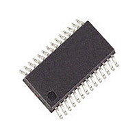
DS90LV110ATMT National Semiconductor, DS90LV110ATMT Datasheet - Page 3

DS90LV110ATMT
Manufacturer Part Number
DS90LV110ATMT
Description
Manufacturer
National Semiconductor
Datasheet
1.DS90LV110ATMT.pdf
(12 pages)
Specifications of DS90LV110ATMT
Number Of Elements
1
Input Type
CMOS/TTL
Operating Supply Voltage (typ)
3.3V
Differential Input High Threshold Voltage
100mV
Diff. Input Low Threshold Volt
-100mV
Output Type
Repeater
Differential Output Voltage
450mV
Transmission Data Rate
400Mbps
Propagation Delay Time
3.9ns
Power Dissipation
1.209W
Operating Temp Range
-40C to 85C
Operating Temperature Classification
Industrial
Mounting
Surface Mount
Pin Count
28
Package Type
TSSOP
Number Of Receivers
1
Number Of Drivers
10
Lead Free Status / RoHS Status
Not Compliant
Available stocks
Company
Part Number
Manufacturer
Quantity
Price
Part Number:
DS90LV110ATMT
Manufacturer:
NS/国半
Quantity:
20 000
Company:
Part Number:
DS90LV110ATMT/NOPB
Manufacturer:
NS
Quantity:
321
Company:
Part Number:
DS90LV110ATMTCX/NOPB
Manufacturer:
NS/TI
Quantity:
600
SUPPLY CURRENT
I
I
T
T
T
T
T
T
T
T
T
T
T
T
CCD
CCZ
Symbol
LHT
HLT
DJ
RJ
PLHD
PHLD
SKEW
CCS
PHZ
PLZ
PZH
PZL
Symbol
Note 1: “Absolute Maximum Ratings” are these beyond which the safety of the device cannot be guaranteed. They are not meant to imply that the device should
be operated at these limits. The table of “Electrical Characteristics” provides conditions for actual device operation.
Note 2: All typical are given for V
Note 3: V
Note 4: Only one output can be shorted at a time. Don't exceed the package absolute maximum rating.
AC Electrical Characteristics
Over recommended operating supply and temperature ranges unless otherwise specified.
Note 5: The parameters are guaranteed by design. The limits are based on statistical analysis of the device performance over PVT (process, voltage and
temperature) range.
Note 6: The measurement used the following equipment and test setup: HP8133A pattern/pulse generator), 5 feet of RG-142 cable with DUT test board and
HP83480A (digital scope mainframe) with HP83484A (50GHz scope module). The HP8133A with the RG-142 cable exhibit a T
OS
Total Supply Current
TRI-STATE Supply Current
Output Low-to-High Transition Time, 20% to 80%, Figure 4
(Note 5)
Output High-to-Low Transition Time, 80% to 20%, Figure 4
(Note 5)
LVDS Data Jitter, Deterministic (Peak-to-
Peak) (Note 6)
LVDS Clock Jitter, Random (Note 6)
Propagation Low to High Delay, Figure 5
Propagation High to Low Delay, Figure 5
Pulse Skew |T
Output Channel-to-Channel Skew, Figure 6 (Note 5)
Disable Time (Active to TRI-STATE) High to Z, Figure 1
Disable Time (Active to TRI-STATE) Low to Z, Figure 1
Enable Time (TRI-STATE to Active) Z to High, Figure 1
Enable Time (TRI-STATE to Active) Z to Low, Figure 1
is defined as (V
OH
PLHD
Parameter
+ V
CC
Parameter
OL
= +3.3V and T
- T
) / 2.
PHLD
| (Note 5)
A
= +25°C, unless otherwise stated.
R
EN = High
No Load, 200 MHz, EN = High
EN = Low
L
= 100Ω, C
V
= 1.2V at 400 Mbps (NRZ)
V
at 200 MHz clock
ID
ID
= 300mV; PRBS=2
= 300mV; V
3
L
Conditions
= 5 pF, 200 MHz,
Conditions
CM
= 1.2V
23
-1 data; V
CM
Min
Min
2.2
2.2
DJ
= 26ps and T
10.0
Typ
390
390
145
Typ
125
2.8
2.8
2.8
3.0
1.8
7.0
20
35
80
15
Max
23.0
23.0
RJ
550
550
340
Max
3.6
3.9
6.0
6.0
160
125
91
www.national.com
29
= 1.3 ps
Units
Units
mA
mA
mA
ps
ps
ps
ps
ns
ns
ps
ps
ns
ns
ns
ns


