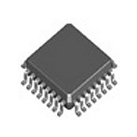
IDTMPC9447AC IDT, Integrated Device Technology Inc, IDTMPC9447AC Datasheet - Page 4

IDTMPC9447AC
Manufacturer Part Number
IDTMPC9447AC
Description
Manufacturer
IDT, Integrated Device Technology Inc
Type
Clock Driverr
Datasheet
1.IDTMPC9447AC.pdf
(10 pages)
Specifications of IDTMPC9447AC
Number Of Clock Inputs
2
Mode Of Operation
Single-Ended
Output Frequency
350MHz
Output Logic Level
LVCMOS
Operating Supply Voltage (min)
2.375V
Operating Supply Voltage (typ)
2.5/3.3V
Operating Supply Voltage (max)
3.465V
Package Type
TQFP
Operating Temp Range
-40C to 85C
Operating Temperature Classification
Industrial
Signal Type
LVCMOS
Mounting
Surface Mount
Pin Count
32
Quiescent Current
2mA
Lead Free Status / RoHS Status
Compliant
Available stocks
Company
Part Number
Manufacturer
Quantity
Price
Part Number:
IDTMPC9447AC
Manufacturer:
IDT
Quantity:
20 000
MPC9447 Data Sheet
Table 6. AC Characteristics (V
Table 7. DC Characteristics (V
MPC9447 REVISION 6 APRIL 13, 2010
1. AC characteristics apply for parallel output termination of 50 Ω to V
2. Violation of the 1.0 ns maximum input rise and fall time limit will affect the device propagation delay, device-to-device skew, reference input pulse width,
3. Setup and hold times are referenced to the falling edge of the selected clock signal input.
4. Output pulse skew is the absolute difference of the propagation delay times: | t
1. The MPC9447 is capable of driving 50 Ω transmission lines on the incident edge. Each output drives one 50 Ω parallel terminated transmission line to a
2. Inputs have pull-down or pull-up resistors affecting the input current.
3. I
Symbol
Symbol
t
t
t
f
PLZ, HZ
PZL, ZH
t
PLH/HL
t
Z
t
sk(PP)
output duty cycle and maximum frequency specifications.
termination voltage of V
P,REF
DC
I
SK(P)
V
f
sk(O)
V
CCQ
t
t
CCQ
t
V
V
max
f
OUT
I
r
r
t
t
JIT
ref
, t
, t
OH
IN
OL
S
H
IH
IL
Q
f
f
is the DC current consumption of the device with all outputs open and the input in its default state or open.
Input Frequency
Output Frequency
Reference Input Pulse Width
CCLK0, CCLK1 Input Rise/Fall Time
Propagation Delay
Output Disable Time
Output Enable Time
Setup Time
Hold Time
Output-to-Output Skew
Device-to-Device Skew
Output Pulse Skew
Output Duty Cycle
Output Rise/Fall Time
Buffer Additive Phase Jitter, RMS
Input High Voltage
Input Low Voltage
Output High Voltage
Output Low Voltage
Output Impedance
Input Current
Maximum Quiescent Supply Current
(2)
TT
. Alternatively, the device drives one 50 Ω series terminated transmission lines per output (V
(4)
Characteristics
Characteristics
CC
CC
CCLK0 or CCLK1 to CLK_STOP
CCLK0 or CCLK1 to CLK_STOP
= 3.3 V ± 5%, T
= 2.5 V ± 5%, T
CCLK0 or CCLK1 to any Q
(3)
A
A
= -40 C to +85 C)
f
= -40 C to +85 C)
Q
<170 MHz
(3)
(3)
TT
.
–0.3
Min
Min
1.4
1.3
0.0
1.0
0.1
1.7
1.8
45
4
0
0
(1)
PLH
– t
PHL
0.03
Typ
Typ
50
19
|.
V
CC
1.0
±300
Max
Max
350
350
150
300
3.3
2.0
1.0
0.7
0.6
2.0
11
11
55
+ 0.3
(2)
3.3V, 2.5V, 1:9 LVCMOS CLOCK FANOUT BUFFER
MHz
MHz
Unit
Unit
mA
µA
ns
ns
ns
ns
ns
ns
ns
ps
ns
ps
ns
ps
%
Ω
V
V
V
V
©2010 Integrated Device Technology, Inc.
CC
LVCMOS
LVCMOS
I
I
V
All V
0.8 to 2.0 V
DC
0.55 to 2.4 V
156.25MHz,
Integration Range:
12kHz - 20MHz
= 2.5 V).
OH
OL
IN
REF
= 15 mA
= –15 mA
= V
CC
CC
= 50%
Pins
or GND
Condition
Condition
(1)


