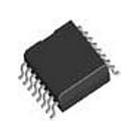
TP3054WM-X National Semiconductor, TP3054WM-X Datasheet - Page 5

TP3054WM-X
Manufacturer Part Number
TP3054WM-X
Description
Manufacturer
National Semiconductor
Type
PCMr
Datasheet
1.TP3054WM-X.pdf
(16 pages)
Specifications of TP3054WM-X
Number Of Channels
1
Number Of Adc's
1
Number Of Dac's
1
Package Type
SOIC W
Interface Type
Serial
Operating Supply Voltage (typ)
±5V
Number Of Adc Inputs
1
Number Of Dac Outputs
1
Operating Supply Voltage (max)
±5.25V
Operating Supply Voltage (min)
±4.75V
Pin Count
16
Mounting
Surface Mount
Lead Free Status / RoHS Status
Not Compliant
Available stocks
Company
Part Number
Manufacturer
Quantity
Price
Part Number:
TP3054WM-X
Manufacturer:
NS/国半
Quantity:
20 000
Part Number:
TP3054WM-X/NOPB
Manufacturer:
NS/国半
Quantity:
20 000
DIGITAL INTERFACE
V
V
V
V
I
I
I
ANALOG INTERFACE WITH TRANSMIT INPUT AMPLIFIER (ALL DEVICES)
I
R
R
R
C
V
A
F
V
V
CMRRXA Common-Mode Rejection Ratio
PSRRXA
ANALOG INTERFACE WITH RECEIVE FILTER (ALL DEVICES)
R
R
C
VOS
POWER DISSIPATION (ALL DEVICES)
I
I
I
I
IL
IH
OZ
I
CC
BB
CC
BB
XA
Symbol
U
IL
IH
OL
OH
O
V
OS
CM
I
O
L
L
O
L
L
Absolute Maximum Ratings
If Military/Aerospace specified devices are required,
please contact the National Semiconductor Sales Office/
Distributors for availability and specifications.
Electrical Characteristics
Unless otherwise noted, limits printed in BOLD characters are guaranteed for V
−40˚C to +85˚C by correlation with 100% electrical testing at T
production tests and/or product design and characterization. All signals referenced to GNDA. Typicals specified at V
+5.0V, V
XA
Note 1: “Absolute Maximum Ratings” indicate limits beyond which damage to the device may occur. Operating Ratings indicate conditions for which the device is
functional, but do not guarantee specific performance limits.
Note 2: I
XA
XA
XA
RF
RF
XA
XA
0
1
V
V
Voltage at any Analog Input
XA
RF
0
1
XA
XA
CC
BB
R
or Output
O
to GNDA
to GNDA
CC0
BB
Input Low Voltage
Input High Voltage
Output Low Voltage
Output High Voltage
Input Low Current
Input High Current
Output Current in High Impedance
State (TRI-STATE)
Input Leakage Current
Input Resistance
Output Resistance
Load Resistance
Load Capacitance
Output Dynamic Range
Voltage Gain
Unity Gain Bandwidth
Offset Voltage
Common-Mode Voltage
Power Supply Rejection Ratio
Output Resistance
Load Resistance
Load Capacitance
Output DC Offset Voltage
Power-Down Current
Power-Down Current
Power-Up (Active) Current
Power-Up (Active) Current
and I
= −5.0V, T
BB0
are measured after first achieving a power-up state.
A
Parameter
= 25˚C.
V
CC
+0.3V to V
(Note 1)
D
SIG
TS
D
SIG
GNDA≤V
V
D
−2.5V≤V≤+2.5V, VF
−2.5V≤V≤+2.5V, VF
Closed Loop, Unity Gain
GS
GS
GS
VF
CMRRXA
DC Test
DC Test
Pin VF
VF
No Load (Note 2)
No Load (Note 2)
No Load( –40˚C to 85˚C)
No Load ( –40˚C to 85˚C)
BB
IH
X
X
X
−0.3V
, I
, I
, GNDA≤V
X
X
R
≤V
X
X
X
R
R
, I
I
O=
−7V
, R
+
L
H
, I
, I
=3.2 mA
7V
L
=−3.2 mA
IN
to GS
R
=3.2 mA, Open Drain
L
H
±
L
≤V
=1.0 mA
O
=−1.0 mA
2.5V
IN
≥ 10 kΩ
CC
>
≤V
X
A
60 dB
5
O
Conditions
IL
= 25˚C. All other limits are assured by correlation with other
≤V
, All Digital Inputs
CC
Voltage at any Digital Input or
Operating Temperature Range
Storage Temperature Range
Lead Temperature
X
X
Output
(Soldering, 10 sec.)
I
I
+
+
or VF
or VF
X
X
CC
I
I
−
−
= +5.0V
±
−200
−200
5000
−2.8
−2.5
Min
−10
−10
−10
−20
600
2.2
2.4
2.4
10
10
60
60
5%, V
1
BB
V
CC
0.65
0.01
Typ
= −5.0V
5.0
5.0
1
2
1
+0.3V to GNDA−0.3V
−55˚C to + 125˚C
−65˚C to +150˚C
±
Max
0.33
11.0
11.0
200
500
200
0.6
0.4
0.4
0.4
2.8
2.5
2.0
10
10
10
50
20
5%; T
3
3
www.national.com
CC
A
300˚C
=
=
Units
MHz
MΩ
V/V
mV
mV
mA
mA
mA
mA
kΩ
µA
µA
µA
nA
pF
dB
dB
pF
Ω
Ω
Ω
V
V
V
V
V
V
V
V
V


