CMF10120D Cree Inc, CMF10120D Datasheet
CMF10120D
Specifications of CMF10120D


Related parts for CMF10120D


CMF10120D Summary of contents
Page 1
... DD t limited J(max) -5/+25 V 152 25°C C -55 to °C +125 1.6mm (0.063”) from case for 10 sec 260 ° 6-32 screw 8.8 lbf-in Subject to change without Notice CMF10120D Pre 1200 160 mΩ DS(On 47.1 nC Package Marking TO-247 CMF10120D Notes , T = 25°C J(max ...
Page 2
... DS = 0V, T =125° 20V 20V 10A D = 20V 10A, T =125° 20V 10A = 20V 10A, T =125° 0V 800V 25mV AC = 800V -2/20V 6.8Ω, = 10A, R G(ext) = 25mV AC Test Conditions Notes = 5A 25° 5A 125° 10A T = 25° Test Conditions Notes 2 CMF10120D Pre. A ...
Page 3
... Fig 2. Typical Output Characteristics T J 1.15 1.1 1.05 1 125C 0.95 25C 0.9 0. Fig 4. Normalized On-Resistance vs. Subject to change without Notice Test Conditions Notes = 800V -2/20V GS 10V 12V 14V 16V 18V 20V ( 125° 100 125 150 Temperature ( C) Temperature 3 CMF10120D Pre. A ...
Page 4
... Fig 6. Transient Thermal Impedance Junction to Case 10000 MHz 1000 100 150 200 Fig 5b. Typical Capacitance vs. VDS (0 - 800V) 1E-3 10E-3 100E-3 Time (sec) Subject to change without Notice MHz C iss C oss C rss 200 400 600 800 V ( CMF10120D Pre. A ...
Page 5
... Gate Charge (nC) Fig 9. Typical Gate Charge Characteristics @ 25°C 400 EON EOFF 350 300 250 200 150 100 50 0 100 125 0 Fig 8. Inductive Switching Energy vs. Drain 40 50 Fig 10. Typical Avalanche Voltage Subject to change without Notice EON EOFF Drain Current (A) Current TBD 5 CMF10120D Pre. A ...
Page 6
... Fig 11. Switching Waveform Test Circuit Fig 13. Body Diode Recovery Waveform Fig 12. Switching Test Waveform Times Fig 14. Body Diode Recovery Test Subject to change without Notice CMF10120D Pre ...
Page 7
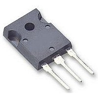
... Copyright © 2006-2009 Cree, Inc. All rights reserved. The information in this document is subject to change without notice. Cree, the Cree logo, and Zero Recovery are registered trademarks of Cree, Inc. Package TO-247-3 Subject to change without Notice 7 CMF10120D Pre. A ...