ICS9DB102BFLFT IDT, Integrated Device Technology Inc, ICS9DB102BFLFT Datasheet - Page 4
ICS9DB102BFLFT
Manufacturer Part Number
ICS9DB102BFLFT
Description
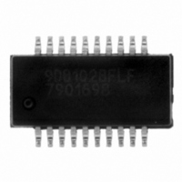
IC BUFFER ZD/FANOUT 20-SSOP
Manufacturer
IDT, Integrated Device Technology Inc
Type
Zero Delay Bufferr
Datasheet
1.ICS9DB102BFLFT.pdf
(13 pages)
Specifications of ICS9DB102BFLFT
Input
Clock
Output
HCSL
Frequency - Max
101MHz
Voltage - Supply
3.135 V ~ 3.465 V
Operating Temperature
0°C ~ 70°C
Mounting Type
Surface Mount
Package / Case
20-SSOP
Frequency-max
101MHz
Lead Free Status / RoHS Status
Lead free / RoHS Compliant
Other names
800-1822-2
9DB102BFLFT
9DB102BFLFT
Available stocks
Company
Part Number
Manufacturer
Quantity
Price
Company:

Part Number:
ICS9DB102BFLFT
Manufacturer:
LTC
Quantity:
108


IDT
T
1
2
3
Electrical Characteristics - PCIEX 0.7V Current Mode Differential Pair
Crossing Voltage (abs) Vcross(abs)
Output-to-Output Skew
Current Source Output
Crossing Voltage (var)
Input to Output Delay
Guaranteed by design, not 100% tested in production.
I
Jitter, Cycle to cycle
A
The 9DB102 does not add a ppm error to the input clock
REF
Absolute min period
Rise Time Variation
ICS9DB102
Two Output Differential Buffer for PCIe Gen1 & Gen2
Fall Time Variation
®
= Tambient; V
Long Accuracy
Two Output Differential Buffer for PCIe Gen1 & Gen2
Average period
PARAMETER
Voltage High
= V
Max Voltage
Voltage Low
Min Voltage
Impedance
Duty Cycle
Rise Time
Fall Time
DD
/(3xR
R
). For R
DD
= 3.3 V +/-5%; C
SYMBOL
t
R
d-Vcross
Tabsmin
jcyc-cycbyp
Tperiod
t
VHigh
= 475 Ω (1%), I
VLow
Vovs
Vuds
jcyc-cyc
t
ppm
pdbyp
d-t
d-t
t
Zo
t
d
sk3
t
t
pd
t3
r
f
r
f
L
=2pF, R
PLL mode. Measurement from
Additve Jitter in Bypass Mode
Measurement on single ended
Measurement from differential
Variation of crossing over all
V
see Tperiod min-max values
V
Statistical measurement on
signal using absolute value.
100.00MHz nominal/spread
OL
single ended signal using
OH
REF
differential wavefrom
100.00MHz nominal
= 0.175V, V
100.00MHz spread
= 0.525V V
= 2.32mA. I
S
CONDITIONS
Bypass mode
=33.2 Ω , R
PLL Mode.
V
wavefrom
V
T
edges
O
= 50%
= V
OL
OH
x
OH
P
= 0.175V
= 0.525V
=49.9 Ω , I
= 6 x I
4
REF
REF
and V
9.9970
9.9970
9.8720
= 475 Ω
3000
MIN
-150
-300
660
250
175
175
3.7
45
0
OH
= 0.7V @ Z
TYP
350
12
30
30
.
10.0030
10.0533
MAX
1150
850
150
550
140
700
700
125
125
150
O
4.2
55
25
35
30
0
=50 Ω .
UNITS NOTES
ppm
mV
mV
mV
mV
ns
ns
ns
ps
ps
ps
ps
ps
ns
ps
ps
ps
%
Ω
852
REV M 01/27/11
1,3
1,3
1,3
1,3
1,3
1,3
1,2
1,2
1
2
2
1
1
1
1
1
1
1
1
1
1
Related parts for ICS9DB102BFLFT
Image
Part Number
Description
Manufacturer
Datasheet
Request
R

Part Number:
Description:
TRANSLATION DEVICE DPI 80-PQFP
Manufacturer:
IDT, Integrated Device Technology Inc
Datasheet:
Part Number:
Description:
IDT PART
Manufacturer:
IDT, Integrated Device Technology Inc
Datasheet:
Part Number:
Description:
IC LIU T1/E1/J1 OCTAL 256PBGA
Manufacturer:
IDT, Integrated Device Technology Inc
Datasheet:

Part Number:
Description:
IC FREQ TIMING GENERATOR 28TSSOP
Manufacturer:
IDT, Integrated Device Technology Inc
Datasheet:
Part Number:
Description:
IC CLK DVR PLL 1:10 40VFQFPN
Manufacturer:
IDT, Integrated Device Technology Inc
Datasheet:
Part Number:
Description:
IC CLK FANOUT BUFFER 1:18 32LQFP
Manufacturer:
IDT, Integrated Device Technology Inc
Datasheet:
Part Number:
Description:
IC CLK FANOUT BUFFER 1:18 32LQFP
Manufacturer:
IDT, Integrated Device Technology Inc
Datasheet:
Part Number:
Description:
IC CK505 VREG/RES 56TSSOP
Manufacturer:
IDT, Integrated Device Technology Inc
Datasheet:

Part Number:
Description:
IC SDRAM CLK DVR 1:10 48-TSSOP
Manufacturer:
IDT, Integrated Device Technology Inc
Datasheet:

Part Number:
Description:
IC CLK DVR PLL 1:10 48TSSOP
Manufacturer:
IDT, Integrated Device Technology Inc
Datasheet:
Part Number:
Description:
IC FLEXPC CLK PROGR P4 56-TSSOP
Manufacturer:
IDT, Integrated Device Technology Inc
Datasheet:
Part Number:
Description:
IC FLEXPC CLK PROGR P4 56-TSSOP
Manufacturer:
IDT, Integrated Device Technology Inc
Datasheet:
Part Number:
Description:
IC FLEXPC CLK PROGR P4 56-SSOP
Manufacturer:
IDT, Integrated Device Technology Inc
Datasheet:

Part Number:
Description:
IC PLL CLK DRIVER 2.5V 28-TSSOP
Manufacturer:
IDT, Integrated Device Technology Inc
Datasheet:
Part Number:
Description:
IC CLOCK DRIVER 2.5V 24-TSSOP
Manufacturer:
IDT, Integrated Device Technology Inc
Datasheet: