ICS9DB106BGLFT IDT, Integrated Device Technology Inc, ICS9DB106BGLFT Datasheet - Page 5
ICS9DB106BGLFT
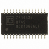
Manufacturer Part Number
ICS9DB106BGLFT
Description
IC BUFFER ZD 6OUTPUT 28-TSSOP
Manufacturer
IDT, Integrated Device Technology Inc
Type
Zero Delay Bufferr
Datasheet
1.ICS9DB106BFLFT.pdf
(14 pages)
Specifications of ICS9DB106BGLFT
Input
Clock
Output
HCSL
Frequency - Max
101MHz
Voltage - Supply
3.135 V ~ 3.465 V
Operating Temperature
0°C ~ 70°C
Mounting Type
Surface Mount
Package / Case
28-TSSOP
Frequency-max
101MHz
Lead Free Status / RoHS Status
Lead free / RoHS Compliant
Other names
800-1242-2
9DB106BGLFT
9DB106BGLFT


IDT
TA = T
Input Slew Rate - DIF_IN
1
2
TA = T
NOTES:
1. Guaranteed by design and characterization, not 100% tested in production.
2. See http://www.pcisig.com for complete specs
3. Device driven by 932S421BGLF or equivalent
4. Measured as maximum pass band gain. At frequencies w ithin the loop BW, highest point of magnification is called PLL jitter peaking.
5. Measured at 3 db dow n or half pow er point.
Electrical Characteristics - Clock Input Parameters
Input Amplitude - DIF_IN
Electrical Characteristics - PLL Parameters
PLL Jitter Peaking
PLL Jitter Peaking
Slew rate measured through +/-75mV window centered around differential zero
Guaranteed by design and characterization, not 100% tested in production.
Input Leakage Current
9DB106
Six Output Differential Buffer for PCIe Gen 2
PLL Bandwidth
PLL Bandwidth
Input Common Mode
Input Jitter - Cycle to
®
Input High Voltage -
Input Low Voltage -
Jitter, Phase
Six Output Differential Buffer for PCIe Gen 2
Voltage - DIF_IN
Input Duty Cycle
PARAMETER
Group
COM
COM
DIF_IN
DIF_IN
Cycle
or T
or T
IND;
IND;
Supply Voltage VDD = 3.3 V +/-5%
Supply Voltage VDD = 3.3 V +/-5%
Parameter
t
j
j
peak-hibw
peak-lobw
pll
jphasePLL
pll
LOBW
HIBW
SYMBOL
V
V
V
V
dv/dt
J
SWING
d
IHDIF
DIFIn
ILDIF
I
COM
IN
tin
(8-16 MHz, 5-16 MHz) Lo-Band <1.5MHz
(8-16 MHz, 5-16 MHz) Hi-Band >1.5MHz
(8-16 MHz, 5-16 MHz) Hi-Band >1.5MHz
Measurement from differential
Common Mode Input Voltage
(single-ended measurement)
(single-ended measurement)
Differential Measurement
Measured differentially
V
Peak to Peak value
PCIe Gen 1 phase jitter
IN
Differential inputs
Differential inputs
CONDITIONS
= V
PCIe Gen 2 jitter
PCIe Gen 2 jitter
PCIe Gen 2 jitter
(PLL_BW = 1)
(PLL_BW = 0)
(PLL_BW = 1)
(PLL_BW = 0)
(1.5 - 22 MHz)
wavefrom
(PLL_BW=1)
(PLL_BW=0)
Description
DD ,
V
IN
= GND
5
V
SS
MIN
600
300
300
0.4
45
-5
0
- 300
Min
0.4
0
0
2
TYP
800
0
Typ
2.5
0.5
2.7
2.2
1.3
40
1
1
MAX
1150
1000
1450
Max
300
125
108
2.5
3.1
3.1
9DB106
55
8
5
2
3
1
3
ps rms
ps rms
ps rms
Units
MHz
MHz
dB
dB
UNITS NOTES
ps
V/ns
mV
mV
mV
mV
uA
ps
REV J 01/27/11
%
Notes
1,2,3
1,2,3
1,2,3
1,2,3
1,4
1,4
1,5
1,5
1,2
1
1
1
1
1
1
1
Related parts for ICS9DB106BGLFT
Image
Part Number
Description
Manufacturer
Datasheet
Request
R

Part Number:
Description:
TRANSLATION DEVICE DPI 80-PQFP
Manufacturer:
IDT, Integrated Device Technology Inc
Datasheet:
Part Number:
Description:
IDT PART
Manufacturer:
IDT, Integrated Device Technology Inc
Datasheet:
Part Number:
Description:
IC LIU T1/E1/J1 OCTAL 256PBGA
Manufacturer:
IDT, Integrated Device Technology Inc
Datasheet:

Part Number:
Description:
IC FREQ TIMING GENERATOR 28TSSOP
Manufacturer:
IDT, Integrated Device Technology Inc
Datasheet:
Part Number:
Description:
IC CLK DVR PLL 1:10 40VFQFPN
Manufacturer:
IDT, Integrated Device Technology Inc
Datasheet:
Part Number:
Description:
IC CLK FANOUT BUFFER 1:18 32LQFP
Manufacturer:
IDT, Integrated Device Technology Inc
Datasheet:
Part Number:
Description:
IC CLK FANOUT BUFFER 1:18 32LQFP
Manufacturer:
IDT, Integrated Device Technology Inc
Datasheet:
Part Number:
Description:
IC CK505 VREG/RES 56TSSOP
Manufacturer:
IDT, Integrated Device Technology Inc
Datasheet:

Part Number:
Description:
IC SDRAM CLK DVR 1:10 48-TSSOP
Manufacturer:
IDT, Integrated Device Technology Inc
Datasheet:

Part Number:
Description:
IC CLK DVR PLL 1:10 48TSSOP
Manufacturer:
IDT, Integrated Device Technology Inc
Datasheet:
Part Number:
Description:
IC FLEXPC CLK PROGR P4 56-TSSOP
Manufacturer:
IDT, Integrated Device Technology Inc
Datasheet:
Part Number:
Description:
IC FLEXPC CLK PROGR P4 56-TSSOP
Manufacturer:
IDT, Integrated Device Technology Inc
Datasheet:
Part Number:
Description:
IC FLEXPC CLK PROGR P4 56-SSOP
Manufacturer:
IDT, Integrated Device Technology Inc
Datasheet:

Part Number:
Description:
IC PLL CLK DRIVER 2.5V 28-TSSOP
Manufacturer:
IDT, Integrated Device Technology Inc
Datasheet:
Part Number:
Description:
IC CLOCK DRIVER 2.5V 24-TSSOP
Manufacturer:
IDT, Integrated Device Technology Inc
Datasheet: