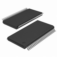
ICS9LPRS436CGLF IDT, Integrated Device Technology Inc, ICS9LPRS436CGLF Datasheet - Page 9

ICS9LPRS436CGLF
Manufacturer Part Number
ICS9LPRS436CGLF
Description
IC CLK SYNTHESIZER 48TSSOP
Manufacturer
IDT, Integrated Device Technology Inc
Datasheet
1.ICS9LPRS436CGLF.pdf
(20 pages)
Specifications of ICS9LPRS436CGLF
Input
*
Output
*
Frequency - Max
*
Voltage - Supply
*
Operating Temperature
*
Mounting Type
Surface Mount
Package / Case
48-TSSOP
Frequency-max
*
Lead Free Status / RoHS Status
Lead free / RoHS Compliant
Other names
800-1933
IDT
1
2
3
4
5
6
*T
AC Electrical Characteristics - Input/Common Parameters
AC Electrical Characteristics - CPU, PCIEX, SATA, DOT96MHz
Electrical Characteristics - PCICLK/PCICLK_F
Guaranteed by design and characterization, not 100% tested in production.
All Long Term Accuracy and Clock Period specifications are guaranteed assuming that REFOUT is at 14.31818MHz
Slew rate emastured through V_swing voltage range centered about differential zero
Vcross is defined at the voltage where Clock = Clock#.
Only applies to the differential rising edge (Clock rising, Clock# falling.)
CPU group skew is nominally 0ps.
A
ICS9LPRS436C
Low Power Clock for Intel Atom
= 0 - 70°C; V
®
Low Power Clock for Intel Atom
SATA Jitter - Cycle to Cycle
CPU Jitter - Cycle to Cycle
SRC Jitter - Cycle to Cycle
DOT Jitter - Cycle to Cycle
Maximum Output Voltage
Differential Voltage Swing
Minimum Output Voltage
Absolute min/max period
Crossing Point Variation
Falling Edge Slew Rate
Rising Edge Slew Rate
Crossing Point Voltage
Rising Edge Slew Rate
Falling Edge Slew Rate
Jitter, Cycle to cycle
DD
CPU[2_ITP:0] Skew
Output High Voltage
Slew Rate Variation
Output High Current
Tdrive_PEREQ_off
Tdrive_PEREQ_on
Output Low Voltage
Output Low Current
Output Impedance
Clk Stabilization
= 3.3 V +/-5%; C
Pin to Pin Skew
CPU[1:0] Skew
Long Accuracy
PARAMETER
Tdrive_PCIEX
PARAMETER
PARAMETER
Tdrive_CPU
Clock period
Tdrive_PD#
Duty Cycle
SRC Skew
Duty Cycle
Trise_SE
Tfall_SE
L
=5pF, Rs=22Ω (unless specified otherwise)
®
-Based Systems
CPUSKEW10
CPUSKEW20
®
VXABSVAR
SATAJC2C
SRCSKEW
-Based Systems
CPUJC2C
SRCJC2C
DOTJC2C
SYMBOL
T
SYMBOL
SYMBOL
VSWING
T
T
tSLVAR
VXABS
DRPEROFF
T
VHIGH
VLOW
t
DCYC
DRPERON
T
T
T
DRPCIEX
jcyc-cyc
T
T
tSLR
tFLR
R
ppm
t
DRSRC
T
V
V
t
t
DRPD
period
I
I
skew
STAB
d
FALL
RISE
SLR
FLR
DSP
OH
OL
abs
OH
OL
t1
From VDD Power-Up or de-assertion of PD to
Fall/rise time of all 3.3V control inputs from
Output stop after PEREQ# deasserted
Output run after PEREQ# asserted
PCI&PCIEX_STOP# de-assertion
33.33MHz output nominal/spread
Differential output enable after
see Tperiod min-max values
Single-ended Measurement
Single-ended Measurement
Single-ended Measurement
33.33MHz output no spread
33.33MHz output no spread
Measured from 0.8 to 2.0 V
Measured from 2.0 to 0.8 V
CPU_STOP# de-assertion
PCIEX output enable after
Differential Measurement
Differential Measurement
Differential Measurement
Differential Measurement
Differential Measurement
Differential Measurement
Differential Measurement
Differential Measurement
Differential Measurement
Differential Measurement
Differential Measurement
33.33MHz output spread
CPU output enable after
V
V
V
Includes undershoot
Includes overshoot
V
OH
PD# de-assertion
OL
OL
OH
V
CONDITIONS
CONDITIONS
CONDITIONS
@MAX = 3.135 V
@ MIN = 1.95 V
@ MAX = 0.4 V
I
O
I
V
V
V
OH
OL
@MIN = 1.0 V
1st clock
20-80%
= V
T
T
T
9
= -1 mA
= 1.5 V
= 1.5 V
= 1.5 V
= 1 mA
DD
*(0.5)
29.99700
30.08421
29.49700
29.56617
MIN
MIN
-300
MIN
-100
300
300
2.5
2.5
-33
2.4
45
30
12
45
1
1
TYP
TYP
TYP
30.00300
30.23459
30.50300
30.58421
MAX
MAX
1150
MAX
300
550
140
125
125
250
100
150
250
100
250
500
1.8
0.4
-33
10
15
10
10
20
55
85
38
55
55
3
3
4
4
4
4
UNITS
UNITS NOTES
clocks
clocks
UNITS NOTES
V/ns
V/ns
V/ns
V/ns
ppm
mV
mV
mV
mV
mV
mA
mA
mA
mA
ms
ns
ns
ns
ns
us
ps
ps
ps
ps
ps
ps
ps
ns
ns
ns
ns
ps
ps
%
%
%
Ω
V
V
1561A — 06/01/10
Notes
1,3,4
1,3,5
1,2
1,2
1,6
1,6
1
1
1
1
1
1
1
1
1
1
1
1
1
2
2
2
2
2
1
1
1
1
1
1
1
1
1
1
1


