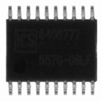
ICS557G-06LF IDT, Integrated Device Technology Inc, ICS557G-06LF Datasheet - Page 8

ICS557G-06LF
Manufacturer Part Number
ICS557G-06LF
Description
IC CLK BUFFER 1:4 HCSL 20-TSSOP
Manufacturer
IDT, Integrated Device Technology Inc
Type
Clock Bufferr
Datasheet
1.ICS557G-06LF.pdf
(11 pages)
Specifications of ICS557G-06LF
Input
HCSL, LVDS
Output
HCSL, LVDS
Frequency - Max
200MHz
Voltage - Supply
3.135 V ~ 3.465 V
Operating Temperature
0°C ~ 70°C
Mounting Type
Surface Mount
Package / Case
20-TSSOP
Frequency-max
200MHz
Number Of Clock Inputs
2
Mode Of Operation
Differential
Output Logic Level
HCSL/LVDS
Operating Supply Voltage (min)
3.135V
Operating Supply Voltage (typ)
3.3V
Operating Supply Voltage (max)
3.465V
Package Type
TSSOP
Operating Temp Range
0C to 70C
Operating Temperature Classification
Commercial
Signal Type
HCSL/LVDS
Mounting
Surface Mount
Pin Count
20
Lead Free Status / RoHS Status
Lead free / RoHS Compliant
Other names
557G-06LF
800-1064
800-1064-5
800-1064
800-1064
800-1064-5
800-1064
Available stocks
Company
Part Number
Manufacturer
Quantity
Price
Company:
Part Number:
ICS557G-06LF
Manufacturer:
IDT
Quantity:
2 006
Part Number:
ICS557G-06LFT
Manufacturer:
IDT
Quantity:
20 000
AC Electrical Characteristics - CLKOUTA/CLKOUTB
Unless stated otherwise, VDD=3.3 V ±5%, Ambient Temperature -40 to +85° C
IDT® 2 TO 4 DIFFERENTIAL CLOCK MUX
Input Frequency
Output Frequency
Input High Voltage
Input Low Voltage
Differential Input
Voltages
Input Offset Voltage
Output High Voltage
Output Low Voltage
Crossing Point
Voltage
Crossing Point
Voltage
Jitter, Cycle-to-Cycle
Rise Time
Fall Time
Rise/Fall Time
Variation
Skew between Outputs
Duty Cycle
Output Enable Time
Output Disable Time
Input to Output Delay
ICS557-06
2 TO 4 DIFFERENTIAL CLOCK MUX
Parameter
1
2
3
4
5
PD = low.
1,2
1,2,4
Test setup is R
Measurement taken from a single-ended waveform.
Measurement taken from a differential waveform.
Measured at the crossing point where instantaneous voltages of both CLKOUT and CLKOUT are equal.
CLKOUT pins are tri-stated when OE is Low asserted. CLKOUT is driven differential when OE is High unless its
1,2
1,2
1,2
1,3
1,2
1,2
1,2
1,2
5
5
1,3
L
=50 ohms with 2 pF, Rr = 475Ω (1%).
Symbol
(V
(V
V
V
V
t
V
t
OR
OF
OH
OL
IH
ID
IS
IL
)
)
HCSL termination
LVDS termination
HCSL
HCSL
LVDS
LVDS
HCSL
HCSL
Absolute
Variation over all edges
From 0.175 V to 0.525 V
From 0.525 V to 0.175 V
Measured at crossing point
All outputs
All outputs
Input differential clock to output
differential clock delay measured at
mid point of input levels to mid pint of
output levels
Conditions
8
1.125
Min.
-150
-150
660
250
660
250
175
175
45
Typ.
1.25
700
350
700
350
332
344
60
10
10
0
0
3
PCIE FAN OUT BUFFER
ICS557-06
1.375
Max.
200
200
100
850
450
850
550
140
700
700
125
27
50
55
Units
MHz
MHz
mV
mV
mV
mV
mV
mV
mV
ps
ps
ps
ps
ps
us
us
ns
%
V
REV J 121510


