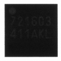
ICS9DBL411AKLFT IDT, Integrated Device Technology Inc, ICS9DBL411AKLFT Datasheet - Page 4

ICS9DBL411AKLFT
Manufacturer Part Number
ICS9DBL411AKLFT
Description
IC FANOUT BUFFER 4OUTPUT 20-MLF
Manufacturer
IDT, Integrated Device Technology Inc
Type
Fanout Bufferr
Datasheet
1.ICS9DBL411AKLFT.pdf
(9 pages)
Specifications of ICS9DBL411AKLFT
Input
Differential
Output
Differential
Frequency - Max
400MHz
Voltage - Supply
3.135 V ~ 3.465 V
Operating Temperature
0°C ~ 70°C
Mounting Type
Surface Mount
Package / Case
20-MLF®, QFN
Frequency-max
400MHz
Number Of Elements
1
Supply Current
54mA
Pll Input Freq (min)
33MHz
Pll Input Freq (max)
400MHz
Operating Supply Voltage (typ)
3.3V
Operating Temp Range
0C to 70C
Package Type
VFQFPN EP
Operating Supply Voltage (min)
3.135V
Operating Supply Voltage (max)
3.465V
Operating Temperature Classification
Commercial
Pin Count
20
Lead Free Status / RoHS Status
Lead free / RoHS Compliant
Other names
800-1824-2
9DBL411AKLFT
9DBL411AKLFT
Available stocks
Company
Part Number
Manufacturer
Quantity
Price
Company:
Part Number:
ICS9DBL411AKLFT
Manufacturer:
VISHAY
Quantity:
17 087
MLF Pin Description
IDT
ICS9DBL411A
Four Output Differential Buffer for PCI Express
(MLF)
PIN #
TM
10
11
12
13
14
15
16
17
18
19
20
1
2
3
4
5
6
7
8
9
Four Output Differential Buffer for PCI Express
VDDA
GNDA
OE3#
DIF3C_LPR
DIF3T_LPR
VDD_IO
GND
DIF2C_LPR
DIF2T_LPR
OE2#
DIF1C_LPR
DIF1T_LPR
OE1#
GND
VDD_IO
DIF0C_LPR
DIF0T_LPR
OE0#
DIF_INC
DIF_INT
PIN NAME
PIN TYPE
PWR
PWR
PWR
GND
GND
GND
OUT
OUT
OUT
OUT
OUT
OUT
OUT
OUT
IN
IN
IN
IN
IN
IN
3.3V Power for the Analog Core
Ground for the Analog Core
Output Enable for DIF3 output. Control is as follows:
0 = enabled, 1 = Low-Low
Complement clock of low power differential clock pair. (no 50ohm shunt resistor to
GND needed)
True clock of low power differential clock pair. (no 50ohm shunt resistor to GND
needed)
Power supply for low power differential outputs, nominal 1.05V to 3.3V
Ground pin
Complement clock of low power differential clock pair. (no 50ohm shunt resistor to
GND needed)
True clock of low power differential clock pair. (no 50ohm shunt resistor to GND
needed)
Output Enable for DIF2 output. Control is as follows:
0 = enabled, 1 = Low-Low
Complement clock of low power differential clock pair. (no 50ohm shunt resistor to
GND needed)
True clock of low power differential clock pair. (no 50ohm shunt resistor to GND
needed)
Output Enable for DIF1 output. Control is as follows:
0 = enabled, 1 = Low-Low
Ground pin
Power supply for low power differential outputs, nominal 1.05V to 3.3V
Complement clock of low power differential clock pair. (no 50ohm shunt resistor to
GND needed)
True clock of low power differential clock pair. (no 50ohm shunt resistor to GND
needed)
Output Enable for DIF0 output. Control is as follows:
0 = enabled, 1 = Low-Low
Complement side of differential input clock
True side of differential input clock
4
DESCRIPTION
Advance Information
1250B—02/21/08


