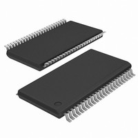
ICS95V857CGLF IDT, Integrated Device Technology Inc, ICS95V857CGLF Datasheet - Page 5

ICS95V857CGLF
Manufacturer Part Number
ICS95V857CGLF
Description
IC CLK DVR PLL 1:10 48TSSOP
Manufacturer
IDT, Integrated Device Technology Inc
Type
PLL Clock Driverr
Datasheet
1.ICS95V857CGLFT.pdf
(13 pages)
Specifications of ICS95V857CGLF
Input
Clock
Output
SSTL-2
Frequency - Max
233MHz
Voltage - Supply
2.3 V ~ 2.7 V
Operating Temperature
0°C ~ 70°C
Mounting Type
Surface Mount
Package / Case
48-TSSOP
Frequency-max
233MHz
Lead Free Status / RoHS Status
Lead free / RoHS Compliant
Other names
95V857CGLF
Notes:
1.
2. DC input signal voltage specifies the allowable DC execution of differential input.
3. Differential inputs signal voltages specifies the differential voltage [VTR-VCP]
4. Differential cross-point voltage is expected to track variations of V
1190A—12/16/05
T
Supply Voltage
Low level input voltage
High level input voltage
DC input signal voltage
(note 2)
Differential input signal
voltage (note 3)
Output differential cross-
voltage (note 4)
Input differential cross-
voltage (note 4)
High level output
current
Low level output current
Operating free-air
temperature
Recommended Operating Condition (see note1)
A
= 0 - 85°C; Supply Voltage AVDD, VDD = 2.5 V +/- 0.2V (unless otherwise stated)
Unused inputs must be held high or low to prevent them from floating.
required for switching, where VT is the true input level and VCP is the
complementary input level.
voltage at which the differential signal must be crossing.
PARAMETER
V
SYMBOL
DD
V
V
V
V
V
V
I
I
, A
T
OH
OL
OX
IH
IN
ID
IX
IL
A
VDD
CLKT, CLKC, FB_INC
PD#
CLKT, CLKC, FB_INC
PD#
DC - CLKT, FB_INT
AC - CLKT, FB_INT
CONDITIONS
5
V
V
DD
V
DD
DD
DD
/2 + 0.18
and is the
/2 - 0.15
0.36
MIN
-0.3
-0.3
/2 - 0.2
2.3
1.7
0.7
0
V
TYP
2.5
0.4
2.1
DD
/2
ICS95V857C
V
V
V
V
V
V
DD
V
DD
DD
DD
DD
DD
DD
/2 + 0.15
MAX
/2 - 0.18
/2 + 0.2
-6.4
2.7
0.7
5.5
85
+ 0.6
+ 0.3
+ 0.6
+ 0.6
UNITS
mA
mA
°C
V
V
V
V
V
V
V
V
V
V


