LMX2512LQX0967 National Semiconductor, LMX2512LQX0967 Datasheet - Page 8
LMX2512LQX0967
Manufacturer Part Number
LMX2512LQX0967
Description
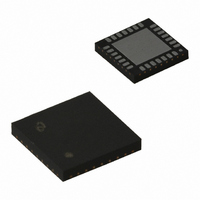
IC SYNTHESIZER PLL VCO 28-LLP
Manufacturer
National Semiconductor
Series
PLLatinum™r
Type
Frequency Synthesizer (RF/IF), Korean CDMA, Cellularr
Datasheet
1.LMX2512LQ0967NOPB.pdf
(18 pages)
Specifications of LMX2512LQX0967
Output
LVCMOS
Frequency - Max
979MHz
Voltage - Supply
2.7 V ~ 3.3 V
Operating Temperature
-30°C ~ 85°C
Mounting Type
Surface Mount
Package / Case
28-LLP
Frequency-max
979MHz
Lead Free Status / RoHS Status
Lead free / RoHS Compliant
Input
-
Available stocks
Company
Part Number
Manufacturer
Quantity
Price
Company:

Part Number:
LMX2512LQX0967
Manufacturer:
SAMTEC
Quantity:
9 023


www.national.com
Functional Description
X = Don’t care.
LOCK DETECT
The LD output can be used to indicate the lock status of the
RF PLL. Bit 21 in Register R0 determines the signal that
appears on the LD pin. When the RF PLL is not locked, the
Note 9: LD output becomes LOW when the phase error is larger than t
Note 10: LD output becomes HIGH when the phase error is less than t
four or more consecutive cycles.
Note 11: Phase Error is measured on leading edge. Only errors greater than
t
W1
CE Pin
and t
0
1
1
1
1
W2
TABLE 2. Power Down Configuration
are labeled.
RF_EN
X
0
0
1
1
IF_EN
FIGURE 1. Lock Detect Timing Diagram Waveform (Notes 9, 10, 11, 12, 13)
X
0
1
0
1
RF Circuitry
OFF
OFF
OFF
ON
ON
(Continued)
IF Circuitry
OFF
OFF
OFF
ON
ON
W1
W2
for
.
8
LD pin remains LOW. After obtaining phase lock, the LD pin
will have a logical HIGH level. The output can also be
programmed to be ground at all times.
Note 12: t
Note 13: The lock detect comparison occurs with every 64
f
N
.
RF PLL Section
W1
LD Bit
Not Locked
and t
0
1
Locked
TABLE 3. Lock Detect Modes
TABLE 4. Lock Detect Logic
W2
are equal to 10 ns.
Disable (GND)
Enable
Mode
LD Output
HIGH
LOW
20068005
th
cycle of f
R
and
Related parts for LMX2512LQX0967
Image
Part Number
Description
Manufacturer
Datasheet
Request
R

Part Number:
Description:
National Semiconductor [8-Bit D/A Converter]
Manufacturer:
National Semiconductor
Datasheet:
Part Number:
Description:
National Semiconductor [Media Coprocessor]
Manufacturer:
National Semiconductor
Datasheet:
Part Number:
Description:
Digitally Controlled Tone and Volume Circuit with Stereo Audio Power Amplifier, Microphone Preamp Stage and National 3D Sound
Manufacturer:
National Semiconductor
Datasheet:
Part Number:
Description:
Digitally Controlled Tone and Volume Circuit with Stereo Audio Power Amplifier, Microphone Preamp Stage and National 3D Sound
Manufacturer:
National Semiconductor
Datasheet:
Part Number:
Description:
AC97 Rev 2 Codec with Sample Rate Conversion and National 3D Sound
Manufacturer:
National Semiconductor
Part Number:
Description:
Manufacturer:
National Semiconductor
Datasheet:
Part Number:
Description:
Manufacturer:
National Semiconductor
Datasheet:
Part Number:
Description:
General Purpose, Low Voltage, Low Power, Rail-to-Rail Output Operational Amplifiers
Manufacturer:
National Semiconductor
Datasheet:
Part Number:
Description:
8-bit 20 MSPS flash A/D converter.
Manufacturer:
National Semiconductor
Datasheet:
Part Number:
Description:
Low Noise Quad Operational Amplifier
Manufacturer:
National Semiconductor
Datasheet:
Part Number:
Description:
Quad Differential Line Receivers
Manufacturer:
National Semiconductor
Datasheet:
Part Number:
Description:
Quad High Speed Trapezoidal? Bus Transceiver
Manufacturer:
National Semiconductor
Datasheet:
Part Number:
Description:
Dual Line Receiver
Manufacturer:
National Semiconductor
Datasheet:
Part Number:
Description:
TTL to 10k ECL Level Translator with Latch
Manufacturer:
National Semiconductor
Datasheet: